
 German
 Japanese
 Portuguese
 Korea
Korea
 Mexico
 Dutch
Dutch


onsemi
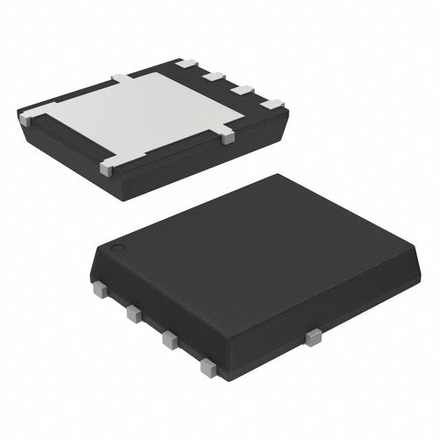
NVMFS5C604NLWFAFT1G

Why Choose Us?
Professional Platform
B2B & B2C purchasingDelivery at full speed
1-2 days deliveryWide variety
Original manufacturers365 days guarantee
Responsible quality
.png)


Tech Specifications
NVMFS5C604NLWFAFT1G Description
NVMFS5C604NLWFAFT1G Description
The NVMFS5C604NLWFAFT1G from onsemi is a high-performance N-channel MOSFET designed for demanding automotive and industrial applications. With a 60V drain-to-source voltage (Vdss) and an impressive continuous drain current (Id) of 287A (Tc), this device delivers robust power handling in a compact 5DFN surface-mount package. Its ultra-low on-resistance (Rds(on)) of 1.2mOhm at 50A, 10V minimizes conduction losses, enhancing efficiency in high-current circuits. The MOSFET is AEC-Q101 qualified, ensuring reliability for automotive environments, and features a ±20V gate-to-source voltage (Vgs) tolerance for robust gate drive compatibility.
NVMFS5C604NLWFAFT1G Features
- Low Rds(on): 1.2mOhm @ 50A, 10V reduces power dissipation and improves thermal performance.
- High Current Capability: 287A (Tc) continuous drain current supports high-power applications.
- Automotive Grade: Compliant with AEC-Q101 standards for harsh operating conditions.
- Optimized Gate Charge: 52nC @ 4.5V (Qg) ensures fast switching and reduced switching losses.
- Wide Vgs Range: ±20V gate drive tolerance enhances design flexibility.
- Advanced Packaging: 5DFN (Tape & Reel) offers space savings and automated assembly compatibility.
- RoHS3 & REACH Compliant: Meets environmental and regulatory requirements.
NVMFS5C604NLWFAFT1G Applications
This MOSFET is ideal for high-efficiency power conversion systems, including:
- Automotive Systems: Electric vehicle (EV) power distribution, motor drives, and battery management.
- Industrial Power Supplies: High-current DC-DC converters, synchronous rectification, and load switches.
- Energy Storage: Solar inverters and UPS systems requiring low-loss switching.
- High-Frequency Switching: Applications demanding fast switching speeds and minimal thermal resistance.
Conclusion of NVMFS5C604NLWFAFT1G
The NVMFS5C604NLWFAFT1G stands out for its exceptional current handling, ultra-low Rds(on), and automotive-grade reliability. Its optimized gate charge and thermal performance make it a superior choice for high-power designs where efficiency and durability are critical. Whether in automotive electrification or industrial power systems, this MOSFET delivers high performance, compact integration, and compliance with stringent industry standards.
FAQ
Not available to buy online? Want the lower wholesale price? Please Send RFQ to get best price, we will respond immediately


.png?x-oss-process=image/format,webp/resize,h_32)


