

onsemi
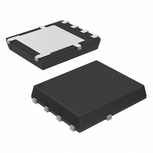
NVMFS5C612NLAFT1G
Single FETs, MOSFETs

Not available to buy online? Want the lower wholesale price? Please Send RFQ to get best price, we will respond immediately


.png?x-oss-process=image/format,webp/resize,p_30)


NVMFS5C612NLAFT1G Description
The NVMFS5C612NLAFT1G is a high-performance MOSFET (Metal-Oxide-Semiconductor Field-Effect Transistor) manufactured by ON Semiconductor. It is designed for use in a variety of power electronic applications, including motor control, power supplies, and renewable energy systems.
Description:
The NVMFS5C612NLAFT1G is a N-channel MOSFET with a drain-to-source voltage (VDS) of 600V and a continuous drain current (ID) of 12.5A. It is available in a TO-220 package, which is suitable for both through-hole and surface-mount applications.
Features:
- High voltage and current ratings: The NVMFS5C612NLAFT1G is designed to handle high voltages and currents, making it suitable for use in demanding power electronic applications.
- Low on-state resistance (RDS(on)): The device has a low on-state resistance, which helps to minimize power losses and improve efficiency.
- Fast switching speed: The MOSFET has a fast switching speed, which allows it to operate effectively in high-frequency applications.
- High thermal stability: The device is designed to operate reliably at high temperatures, making it suitable for use in harsh environments.
- Integrated protection features: The NVMFS5C612NLAFT1G includes built-in protection features, such as over-voltage, over-current, and over-temperature protection, to ensure reliable operation.
Applications:
The NVMFS5C612NLAFT1G is suitable for use in a variety of power electronic applications, including:
- Motor control: The MOSFET can be used in motor control applications, such as in industrial automation systems and electric vehicles.
- Power supplies: The device is suitable for use in power supply applications, such as in switching power supplies and battery chargers.
- Renewable energy systems: The NVMFS5C612NLAFT1G can be used in renewable energy systems, such as solar panel inverters and wind turbine power converters.
- Lighting systems: The MOSFET can be used in lighting systems, such as LED drivers and fluorescent lamp ballasts.
- Industrial control systems: The device is suitable for use in industrial control systems, such as in programmable logic controllers (PLCs) and variable frequency drives (VFDs).
In summary, the NVMFS5C612NLAFT1G is a high-performance MOSFET that offers a combination of high voltage and current ratings, low on-state resistance, fast switching speed, and integrated protection features. It is suitable for use in a wide range of power electronic applications, including motor control, power supplies, renewable energy systems, lighting systems, and industrial control systems.
Tech Specifications
NVMFS5C612NLAFT1G Documents
Download datasheets and manufacturer documentation for NVMFS5C612NLAFT1G
Wafer Fab 19/Feb/2021 NVMFS5C612NL MPN Label Update 08/Sep/2021 MPN label update 11/Oct/2021 NVMFS5C612NL onsemi RoHS Material Declaration NVMFS5C612NLAFT1G onsemi REACH Related Parts


Shopping Guide


.png?x-oss-process=image/format,webp/resize,h_32)


©2025 ERSA Electronics Corporation.