
 German
 Japanese
 Portuguese
 Korea
Korea
 Mexico
 Dutch
Dutch


onsemi
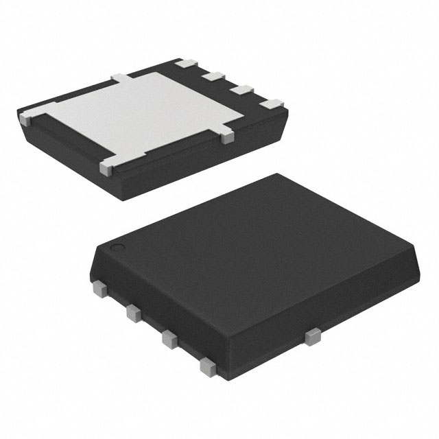
NVMFS5C673NLWFAFT1G

Why Choose Us?
Professional Platform
B2B & B2C purchasingDelivery at full speed
1-2 days deliveryWide variety
Original manufacturers365 days guarantee
Responsible quality
.png)


Tech Specifications
NVMFS5C673NLWFAFT1G Description
The NVMFS5C673NLWFAFT1G is a high-performance MOSFET (Metal-Oxide-Semiconductor Field-Effect Transistor) manufactured by ON Semiconductor. It is designed for use in a wide range of applications, including power switching, motor control, and power management.
Description:
The NVMFS5C673NLWFAFT1G is a N-channel MOSFET with an Rds(on) of 67mΩ and a maximum drain-source voltage (Vds) of 100V. It is available in a TO-220 package, making it suitable for use in a variety of power electronic circuits.
Features:
- Low Rds(on): The low on-state resistance of the NVMFS5C673NLWFAFT1G allows for efficient power switching with minimal power loss.
- High Vds: The high maximum drain-source voltage rating of 100V makes the NVMFS5C673NLWFAFT1G suitable for use in high voltage applications.
- High Current Capability: The NVMFS5C673NLWFAFT1G can handle a continuous drain current of up to 54A, making it suitable for use in high current applications.
- Thermally Efficient Package: The TO-220 package is designed to provide good thermal performance, allowing for efficient heat dissipation and improved reliability.
Applications:
- Power Switching: The NVMFS5C673NLWFAFT1G can be used in power switching applications, such as DC-DC converters and power supplies.
- Motor Control: The high current capability and low on-state resistance of the NVMFS5C673NLWFAFT1G make it suitable for use in motor control applications, such as brushless DC motor drivers.
- Power Management: The NVMFS5C673NLWFAFT1G can be used in power management applications, such as battery management systems and solar power inverters.
Overall, the NVMFS5C673NLWFAFT1G is a versatile and high-performance MOSFET that can be used in a wide range of power electronic applications. Its low on-state resistance, high voltage rating, and high current capability make it an ideal choice for power switching, motor control, and power management applications.
FAQ
| Quantity | Unit Price | Ext. Price |
|---|---|---|
| 1+ | $2.14457 | $2.14 |
| 10+ | $1.81885 | $18.19 |
| 30+ | $1.61657 | $48.50 |
Not available to buy online? Want the lower wholesale price? Please Send RFQ to get best price, we will respond immediately


.png?x-oss-process=image/format,webp/resize,h_32)


