
 German
 Japanese
 Portuguese
 Korea
Korea
 Mexico
 Dutch
Dutch


STMicroelectronics
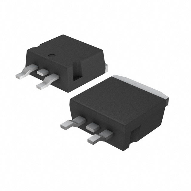
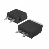
STB40NF10LT4
Why Choose Us?
Professional Platform
B2B & B2C purchasingDelivery at full speed
1-2 days deliveryWide variety
Original manufacturers365 days guarantee
Responsible quality
.png)


Tech Specifications
STB40NF10LT4 Description
STB40NF10LT4 is a high-power N-channel MOSFET transistor manufactured by STMicroelectronics. It is designed for use in a variety of power electronic applications, including motor control, power supplies, and power converters.
Description:
The STB40NF10LT4 is a high-power N-channel MOSFET transistor that features a maximum drain-source voltage (VDS) of 100V and a continuous drain current (ID) of 40A. It is available in a TO-220L package, which is suitable for use in a variety of power electronic applications.
Features:
- N-channel MOSFET transistor
- Maximum drain-source voltage (VDS) of 100V
- Continuous drain current (ID) of 40A
- Low on-state resistance (RDS(on))
- High switching speed
- Low gate charge
- Suitable for use in a wide range of power electronic applications
Applications:
- Motor control
- Power supplies
- Power converters
- Battery management systems
- Inverters
- Switch mode power supplies (SMPS)
- Industrial control systems
The STB40NF10LT4 is a high-power MOSFET transistor that is designed for use in a variety of power electronic applications. Its high current handling capability and low on-state resistance make it an excellent choice for applications that require high efficiency and high power density. Its high switching speed and low gate charge also make it well-suited for use in high-frequency applications. Overall, the STB40NF10LT4 is a versatile and reliable MOSFET transistor that can be used in a wide range of power electronic applications.
FAQ
Not available to buy online? Want the lower wholesale price? Please Send RFQ to get best price, we will respond immediately


.png?x-oss-process=image/format,webp/resize,h_32)


