
 German
 Japanese
 Portuguese
 Korea
Korea
 Mexico
 Dutch
Dutch


STMicroelectronics
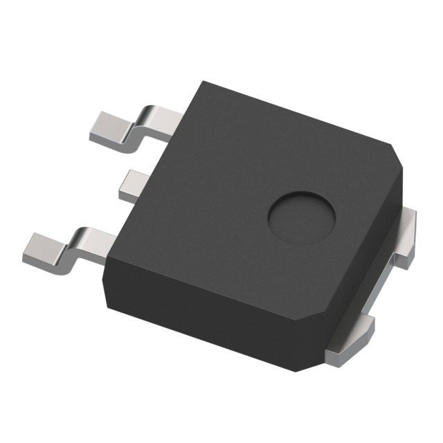
STD10NF30

Why Choose Us?
Professional Platform
B2B & B2C purchasingDelivery at full speed
1-2 days deliveryWide variety
Original manufacturers365 days guarantee
Responsible quality
.png)


Tech Specifications
STD10NF30 Description
STD10NF30 Description
The STD10NF30 is a high-performance N-channel MOSFET from STMicroelectronics, designed for demanding automotive applications. It offers a unique combination of low on-resistance, high input capacitance, and low gate charge, making it ideal for high-efficiency power management in automotive systems. The device is built on STMicroelectronics' advanced MESH OVERLAY™ technology, ensuring superior performance and reliability.
STD10NF30 Features
- Low On-Resistance: The STD10NF30 boasts an ultra-low on-resistance of 330mOhm at 5A and 10V, enabling high-efficiency power conversion and reducing power losses in automotive systems.
- High Input Capacitance: With a maximum input capacitance of 780 pF at 25V, the STD10NF30 offers excellent high-frequency performance, making it suitable for high-speed switching applications.
- Low Gate Charge: The device features a low gate charge of 23 nC at 10V, reducing switching losses and improving overall efficiency.
- Robust Voltage Ratings: The STD10NF30 can handle drain-to-source voltages up to 300V, making it suitable for a wide range of automotive applications.
- Automotive Grade: The device is designed to meet the stringent requirements of the automotive industry, with a maximum power dissipation of 103W at Tc and a moisture sensitivity level of 1 (unlimited).
- Compliance: The STD10NF30 is compliant with the latest RoHS3 standards, ensuring environmental sustainability and regulatory compliance.
STD10NF30 Applications
The STD10NF30 is ideal for a variety of automotive applications, including:
- Power Management: The low on-resistance and high input capacitance make it suitable for high-efficiency power conversion in automotive systems.
- Motor Control: The device's robust voltage ratings and low gate charge make it ideal for motor control applications, such as electric power steering and electric vehicle motor drives.
- LED Lighting: The STD10NF30 can be used in automotive LED lighting systems, providing efficient power management and high-speed switching capabilities.
- Battery Management: The device's low on-resistance and high input capacitance make it suitable for battery management systems in electric and hybrid vehicles.
Conclusion of STD10NF30
The STD10NF30 is a high-performance N-channel MOSFET from STMicroelectronics, designed specifically for demanding automotive applications. Its unique combination of low on-resistance, high input capacitance, and low gate charge, along with its robust voltage ratings and automotive-grade compliance, make it an ideal choice for high-efficiency power management, motor control, LED lighting, and battery management systems in the automotive industry. With its advanced MESH OVERLAY™ technology, the STD10NF30 offers superior performance and reliability, ensuring optimal operation in the most demanding automotive environments.
FAQ
Not available to buy online? Want the lower wholesale price? Please Send RFQ to get best price, we will respond immediately


.png?x-oss-process=image/format,webp/resize,h_32)


