
STMicroelectronics
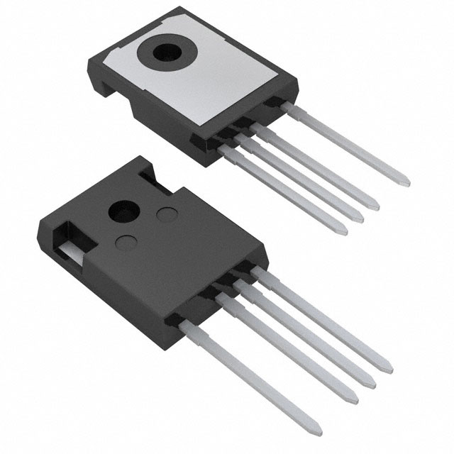
STGW40H65DFB

Why Choose Us?
Professional Platform
B2B & B2C purchasingDelivery at full speed
1-2 days deliveryWide variety
Original manufacturers365 days guarantee
Responsible quality
.png)


Tech Specifications
STGW40H65DFB Description
STMicroelectronics' STGW40H65DFB is a high-voltage, high-power MOSFET (Metal-Oxide-Semiconductor Field-Effect Transistor) designed for use in a variety of industrial and automotive applications. Here is a description of the model, its features, and potential applications:
Model Description:
The STGW40H65DFB is a N-channel MOSFET that is part of the SuperFET family from STMicroelectronics. It is designed to handle high voltage and high power requirements, making it suitable for applications that demand robust and reliable performance.
Features:
-
High Voltage Rating: The device is rated for a maximum drain-source voltage (VDS) of 650V, which allows it to be used in high-voltage applications.
-
High Current Capability: With a continuous drain current (ID) of up to 40A, the STGW40H65DFB can handle significant current loads, making it suitable for power electronics applications.
-
Low On-State Resistance (RDS(on)): The device has a low on-state resistance, which minimizes power dissipation and improves efficiency in switching applications.
-
High-Speed Switching: The MOSFET is designed for fast switching, which is crucial for applications that require quick response times.
-
Robust Construction: The SuperFET technology used in the STGW40H65DFB provides a robust and reliable device that can withstand high temperatures and harsh environments.
-
Integrated Protection Features: The device may include built-in protection features such as over-voltage, over-current, and thermal shutdown to protect the MOSFET from damage.
-
Automotive Qualification: The STGW40H65DFB is qualified for use in the automotive industry, adhering to the stringent requirements of automotive electronics.
Applications:
-
Industrial Motor Control: The high voltage and current ratings make the STGW40H65DFB suitable for controlling industrial motors in applications like conveyor systems, machine tools, and robotics.
-
Automotive Applications: Due to its automotive qualification, the MOSFET can be used in various automotive systems, including electric power steering, electric braking systems, and battery management systems.
-
Power Supplies: The device can be used in high-voltage power supply designs, such as switched-mode power supplies (SMPS) and uninterruptible power supplies (UPS).
-
Inverters: The STGW40H65DFB is suitable for use in inverter circuits for renewable energy systems, such as solar panel inverters and variable frequency drives (VFDs).
-
Battery Protection: The MOSFET can be used in battery protection circuits to manage and protect the flow of current in and out of battery systems.
-
High-Voltage Load Switching: For applications that require switching high-voltage loads, such as in lighting systems or high-voltage LED drivers, the STGW40H65DFB is a suitable choice.
Please note that the actual features and specifications of the STGW40H65DFB may vary, and it is essential to refer to the manufacturer's datasheet for detailed information and to ensure that the device meets the requirements of a specific application.
FAQ
| Quantity | Unit Price | Ext. Price |
|---|---|---|
| 1+ | $3.21257 | $3.21 |
| 10+ | $2.70857 | $27.09 |
| 30+ | $2.29715 | $68.91 |
Not available to buy online? Want the lower wholesale price? Please Send RFQ to get best price, we will respond immediately


.png?x-oss-process=image/format,webp/resize,h_32)


