
 German
 Japanese
 Portuguese
 Korea
Korea
 Mexico
 Dutch
Dutch


Texas Instruments
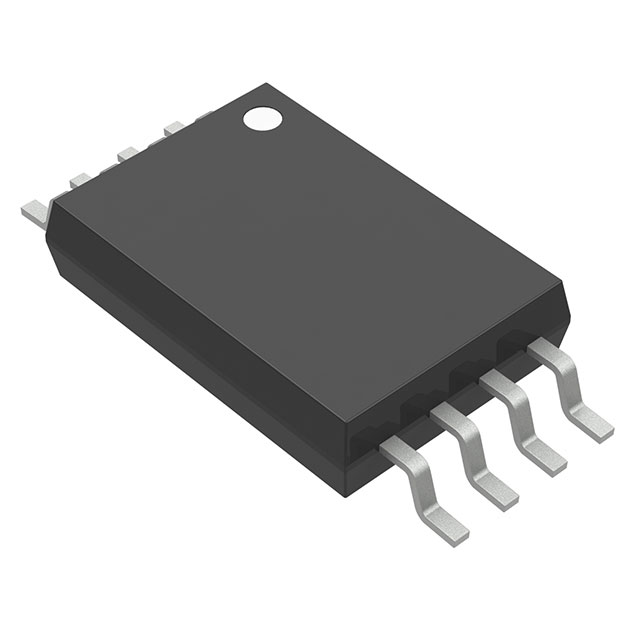
CD40107BPWR

Why Choose Us?
Professional Platform
B2B & B2C purchasingDelivery at full speed
1-2 days deliveryWide variety
Original manufacturers365 days guarantee
Responsible quality
.png)


Tech Specifications
CD40107BPWR Description
CD40107BPWR Description
The CD40107BPWR is a high-performance NAND gate IC designed for a wide range of digital logic applications. Manufactured by Texas Instruments, this device is part of the 4000B series and is known for its robustness and versatility. It features two 2-input NAND gates in an 8-TSSOP package, making it suitable for surface-mount applications. The CD40107BPWR operates within a wide supply voltage range of 3V to 18V, ensuring compatibility with various power supply configurations. It also supports a broad range of input logic levels, with low levels ranging from 1.5V to 4V and high levels from 3.5V to 11V. The device boasts a maximum propagation delay of 100ns at 15V and 50pF, making it ideal for high-speed digital circuits. Additionally, it features open-drain outputs, which allow for flexible circuit design and easy interfacing with other digital components.
CD40107BPWR Features
- Logic Type: NAND Gate
- Number of Circuits: 2
- Number of Inputs per Circuit: 2
- Supply Voltage Range: 3V to 18V
- Input Logic Levels:
- Low: 1.5V to 4V
- High: 3.5V to 11V
- Max Propagation Delay: 100ns @ 15V, 50pF
- Mounting Type: Surface Mount
- Package: 8-TSSOP
- Features: Open Drain
- Current - Quiescent (Max): 4 µA
- Moisture Sensitivity Level (MSL): 1 (Unlimited)
- Compliance:
- ECCN: EAR99
- REACH Status: REACH Unaffected
- RoHS Status: ROHS3 Compliant
- HTSUS: 8542.39.0001
CD40107BPWR Applications
The CD40107BPWR is well-suited for a variety of applications due to its wide operating voltage range and versatile input logic levels. It is ideal for use in digital circuits requiring high-speed switching and low power consumption. Some specific applications include:
- Digital Logic Circuits: The NAND gates can be used to create complex digital logic functions, such as decoders, multiplexers, and flip-flops.
- Control Systems: The open-drain outputs make it suitable for interfacing with microcontrollers and other digital devices, allowing for efficient control and signaling.
- Consumer Electronics: The device's wide voltage range and low quiescent current make it suitable for battery-powered devices and portable electronics.
- Industrial Automation: The robustness and reliability of the CD40107BPWR make it ideal for use in industrial control systems and automation equipment.
Conclusion of CD40107BPWR
The CD40107BPWR is a versatile and reliable NAND gate IC that offers significant advantages over similar models. Its wide operating voltage range, low quiescent current, and open-drain outputs make it suitable for a variety of applications, from digital logic circuits to industrial automation. The device's compliance with industry standards such as REACH and RoHS ensures that it meets environmental and safety regulations. With its high-speed performance and flexible design, the CD40107BPWR is an excellent choice for engineers and designers looking for a robust and efficient digital logic solution.
FAQ
| Quantity | Unit Price | Ext. Price |
|---|---|---|
| 1+ | $0.41360 | $0.41 |
| 10+ | $0.29128 | $2.91 |
| 25+ | $0.26013 | $6.50 |
| 100+ | $0.22581 | $22.58 |
| 250+ | $0.20937 | $52.34 |
Not available to buy online? Want the lower wholesale price? Please Send RFQ to get best price, we will respond immediately


.png?x-oss-process=image/format,webp/resize,h_32)


