
Texas Instruments
CD4013BPWRG4
Flip Flops


.png?x-oss-process=image/format,webp/resize,p_30)


CD4013BPWRG4 Description
CD4013BPWRG4 Description
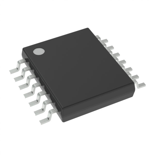
The CD4013BPWRG4 is a dual D-type flip-flop integrated circuit (IC) from Texas Instruments, designed for a wide range of digital applications. This IC is part of the 4000B series and is housed in a 14-TSSOP surface-mount package, making it suitable for compact and high-density PCB designs. The CD4013BPWRG4 operates within a supply voltage range of 3V to 18V, providing flexibility in various power supply environments. It features a maximum clock frequency of 24 MHz, ensuring high-speed operation while maintaining low power consumption with a quiescent current of just 4 µA.
CD4013BPWRG4 Features
- Dual D-Type Flip-Flops: The CD4013BPWRG4 contains two independent D-type flip-flops, each capable of storing a single bit of data. This dual functionality allows for efficient use of space and resources on the PCB.
- Positive Edge Triggering: The flip-flops are triggered on the positive edge of the clock signal, ensuring reliable and predictable data capture.
- Complementary Outputs: Each flip-flop provides complementary outputs, which can be useful for driving various types of digital circuits and reducing the need for additional inverters.
- Set and Reset Functions: The IC includes set (preset) and reset functions, allowing for precise control over the state of the flip-flops. This feature is particularly useful in applications requiring initialization or error recovery.
- Wide Operating Voltage Range: With a supply voltage range of 3V to 18V, the CD4013BPWRG4 can be used in a variety of power supply environments, from low-power battery-operated devices to higher-voltage industrial systems.
- Low Power Consumption: The IC has a low quiescent current of 4 µA, making it suitable for battery-powered and energy-efficient applications.
- High-Speed Operation: The maximum clock frequency of 24 MHz ensures that the CD4013BPWRG4 can handle high-speed data processing tasks.
- Compliance and Reliability: The CD4013BPWRG4 is REACH unaffected and RoHS3 compliant, ensuring that it meets the latest environmental and safety standards. Additionally, its moisture sensitivity level (MSL) is 1 (unlimited), making it suitable for a wide range of manufacturing processes.
CD4013BPWRG4 Applications
The CD4013BPWRG4 is ideal for a variety of applications due to its dual functionality, wide operating voltage range, and low power consumption. Some specific use cases include:
- Digital Counters: The dual D-type flip-flops can be used to build binary counters, which are essential in digital timing and control circuits.
- Data Storage and Transfer: The flip-flops can store and transfer data in digital systems, making them suitable for use in memory elements and data registers.
- Clock Dividers: The CD4013BPWRG4 can be used to divide clock signals, generating lower frequency clock signals for various digital circuits.
- Sequential Logic Circuits: The set and reset functions make this IC ideal for designing sequential logic circuits, such as state machines and shift registers.
- Battery-Powered Devices: The low power consumption and wide operating voltage range make the CD4013BPWRG4 suitable for use in portable and battery-powered devices, where power efficiency is critical.
Conclusion of CD4013BPWRG4
The CD4013BPWRG4 from Texas Instruments is a versatile and reliable dual D-type flip-flop IC, offering a wide range of features and benefits. Its dual functionality, positive edge triggering, complementary outputs, and set/reset functions make it suitable for a variety of digital applications. The wide operating voltage range and low power consumption further enhance its flexibility and efficiency. With its compliance to environmental and safety standards, the CD4013BPWRG4 is an excellent choice for engineers and designers looking for a robust and reliable digital IC for their projects.
Tech Specifications
CD4013BPWRG4 Documents
Download datasheets and manufacturer documentation for CD4013BPWRG4
 Mechanical Outline Drawing
  Qualification of Mold Compound for Select Devices using TSSOP package (PDF)
  CD4013BPWRG4 Symbol & Footprint by SnapMagic
  Logic Guide (Rev. AB)
 Shopping Guide


.png?x-oss-process=image/format,webp/resize,h_32)


