
 German
 Japanese
 Portuguese
 Korea
Korea
 Mexico
 Dutch
Dutch


Texas Instruments
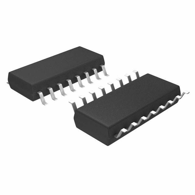
CD40175BNSR

Why Choose Us?
Professional Platform
B2B & B2C purchasingDelivery at full speed
1-2 days deliveryWide variety
Original manufacturers365 days guarantee
Responsible quality
.png)


Tech Specifications
CD40175BNSR Description
CD40175BNSR Description
The CD40175BNSR is a high-performance, single 4-bit D-type flip-flop IC designed by Texas Instruments. This device is part of the 4000B series and is optimized for a wide range of digital applications. It features a complementary output type, positive edge triggering, and a master reset function, making it highly versatile for various digital circuits. The CD40175BNSR operates within a supply voltage range of 3V to 18V and supports a maximum clock frequency of 14 MHz. It is available in a surface-mount package, specifically in a 16SO configuration, and is REACH unaffected and RoHS3 compliant, ensuring environmental and regulatory standards are met.
CD40175BNSR Features
- High Clock Frequency: The CD40175BNSR supports a maximum clock frequency of 14 MHz, enabling fast data processing and high-speed operations.
- Complementary Outputs: This feature ensures robust and reliable signal transmission, making it suitable for applications requiring both true and complement outputs.
- Positive Edge Triggering: The flip-flop is triggered on the positive edge of the clock signal, providing precise timing control and synchronization.
- Wide Operating Voltage Range: With a supply voltage range of 3V to 18V, the CD40175BNSR is highly adaptable to various power supply configurations.
- Low Quiescent Current: The device consumes only 4 µA in quiescent mode, making it energy-efficient and suitable for low-power applications.
- High Output Current: The CD40175BNSR can source and sink up to 6.8 mA, ensuring strong drive capabilities for various loads.
- Master Reset Function: This feature allows for easy initialization and resetting of the flip-flop, simplifying circuit design and operation.
- Moisture Sensitivity Level 1: The device is classified as MSL 1, meaning it is not moisture-sensitive and can be stored and handled without special precautions.
CD40175BNSR Applications
The CD40175BNSR is ideal for a variety of applications due to its high performance and versatile features. Some specific use cases include:
- Digital Systems: The high clock frequency and wide operating voltage range make it suitable for digital systems requiring fast data processing and reliable operation.
- Data Storage and Transfer: The 4-bit D-type flip-flop is perfect for data storage and transfer applications, ensuring accurate and efficient data handling.
- Clock and Timing Circuits: The positive edge triggering and master reset function make it ideal for clock and timing circuits where precise timing control is essential.
- Low-Power Devices: The low quiescent current and wide voltage range make it suitable for low-power devices, such as battery-operated systems and portable electronics.
- Automotive and Industrial Applications: The robust design and compliance with environmental standards make it suitable for demanding automotive and industrial applications.
Conclusion of CD40175BNSR
The CD40175BNSR from Texas Instruments is a high-performance, single 4-bit D-type flip-flop that offers a wide range of technical advantages. Its high clock frequency, complementary outputs, and positive edge triggering make it highly versatile and suitable for various digital applications. The wide operating voltage range, low quiescent current, and high output current ensure it is adaptable and energy-efficient. The master reset function simplifies circuit design, while the moisture sensitivity level 1 classification ensures ease of handling and storage. The CD40175BNSR is an excellent choice for digital systems, data storage, clock and timing circuits, low-power devices, and demanding automotive and industrial applications.
FAQ
| Quantity | Unit Price | Ext. Price |
|---|---|---|
| 1+ | $0.49200 | $0.49 |
| 10+ | $0.48000 | $4.80 |
| 30+ | $0.47143 | $14.14 |
Not available to buy online? Want the lower wholesale price? Please Send RFQ to get best price, we will respond immediately


.png?x-oss-process=image/format,webp/resize,h_32)


