
Texas Instruments
CD4071BE

Why Choose Us?
Professional Platform
B2B & B2C purchasingDelivery at full speed
1-2 days deliveryWide variety
Original manufacturers365 days guarantee
Responsible quality
.png)


Tech Specifications
CD4071BE Description
CD4071BE Description
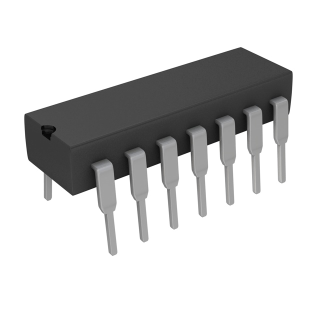
The CD4071BE is a high-performance OR gate designed and manufactured by Texas Instruments. This device is part of the 4000B series and is offered in a 14-pin DIP package. It features 4 independent OR gate circuits, each with 2 inputs, making it ideal for various digital applications that require high-speed signal processing and amplification.
CD4071BE Features
- Logic Type: OR Gate, which is a fundamental building block in digital electronics for combining multiple input signals.
- Max Propagation Delay: 90ns @ 15V, 50pF, ensuring fast signal processing capabilities.
- Voltage - Supply: 3V to 18V, providing flexibility in power supply requirements.
- Input Logic Levels: Low (1.5V to 4V) and High (3.5V to 11V), accommodating a wide range of input voltages.
- Current - Quiescent (Max): 1 µA, indicating low power consumption.
- Current - Output High, Low: 3.4mA, 3.4mA, ensuring consistent output current levels.
- Mounting Type: Through Hole, facilitating easy integration into existing PCB designs.
- Package: Tube, providing protection during storage and handling.
- RoHS Status: ROHS3 Compliant, adhering to environmental regulations.
- REACH Status: REACH Unaffected, indicating compliance with the European Union's regulations on chemicals.
- ECCN: EAR99, for export control classification.
- HTSUS: 8542.39.0001, for harmonized tariff schedules.
- Moisture Sensitivity Level (MSL): Not Applicable, indicating that the device is not sensitive to moisture.
CD4071BE Applications
The CD4071BE is well-suited for a variety of applications where high-speed signal processing and amplification are required. Some specific use cases include:
- Digital Signal Processing: In systems where multiple input signals need to be combined and amplified quickly.
- Automotive Electronics: For processing sensor data in real-time, ensuring reliable and fast response times.
- Industrial Control Systems: In applications requiring the logical combination of multiple input signals for control and monitoring.
- Telecommunications: For signal routing and amplification in data transmission systems.
Conclusion of CD4071BE
The CD4071BE from Texas Instruments stands out for its high-speed performance, low power consumption, and flexibility in input voltage levels. Its 4 independent OR gate circuits make it a versatile choice for a wide range of digital applications. With its RoHS compliance and REACH unaffected status, it is also an environmentally responsible choice. The CD4071BE is an excellent option for designers looking for a reliable and efficient OR gate solution in their next project.
FAQ
| Quantity | Unit Price | Ext. Price |
|---|---|---|
| 1+ | $0.77143 | $0.77 |
| 10+ | $0.63257 | $6.33 |
| 25+ | $0.54000 | $13.50 |
| 100+ | $0.46972 | $46.97 |
| 500+ | $0.42857 | $214.28 |
Not available to buy online? Want the lower wholesale price? Please Send RFQ to get best price, we will respond immediately


.png?x-oss-process=image/format,webp/resize,h_32)


