

Texas Instruments
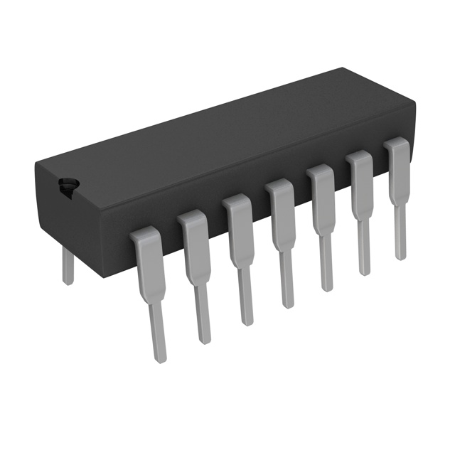
CD4081BE
Gates and Inverters

Not available to buy online? Want the lower wholesale price? Please Send RFQ to get best price, we will respond immediately


- 1+
- $0.71374
- $0.71
- 10+
- $0.58954
- $5.9
- 25+
- $0.48024
- $12.01
- 100+
- $0.41897
- $41.9
- 500+
- $0.38254
- $191.27
- 1000+
- $0.36266
- $362.66

.png?x-oss-process=image/format,webp/resize,p_30)


CD4081BE Description
The Texas Instruments CD4081BE is a high-speed CMOS silicon-gated quad bilateral switch. It is designed for applications that require high-speed switching of analog signals with minimal signal degradation. Here is a description of the model, its features, and applications:
Description:
The CD4081BE is a member of the quad bilateral switch family, which consists of four independent bilateral switches in a single 14-pin DIP (Dual In-line Package) or SOIC (Small Outline Integrated Circuit) package. Each switch is capable of handling both analog and digital signals with high isolation and low cross conduction.
Features:
- High-Speed Operation: The CD4081BE operates at high speeds, making it suitable for applications that require fast switching of analog signals.
- Silicon-Gate CMOS Technology: The use of silicon-gate CMOS technology ensures low power consumption and high reliability.
- High Isolation: The device provides high isolation between channels, minimizing crosstalk and interference.
- Low Cross Conduction: The low cross conduction feature ensures minimal signal degradation when switching between channels.
- Bilateral Switching: Each switch can handle both analog and digital signals, making it versatile for various applications.
- TTL/CMOS Compatible: The device is compatible with both TTL and CMOS logic levels, allowing for easy integration with different types of control circuits.
- 14-Pin DIP or SOIC Package: The CD4081BE is available in both 14-pin DIP and SOIC packages, providing options for different board layouts and space constraints.
Applications:
- Matrix Switching: The CD4081BE can be used in matrix switching applications, where multiple input signals need to be routed to multiple output channels.
- Signal Routing: It is suitable for routing analog and digital signals in communication systems, medical equipment, and test equipment.
- Audio Mixing and Routing: The device can be used in professional audio equipment for mixing and routing audio signals with minimal signal degradation.
- Automotive Applications: The CD4081BE can be used in automotive systems for switching various electronic signals, such as those in infotainment systems or sensor networks.
- Industrial Control Systems: It can be used in industrial control systems for switching and routing signals between different components and sensors.
- Multi-channel Data Acquisition Systems: The CD4081BE can be used in data acquisition systems that require simultaneous switching of multiple analog signals.
In summary, the Texas Instruments CD4081BE is a versatile, high-speed quad bilateral switch that offers excellent performance in various applications requiring the switching and routing of analog and digital signals. Its features, such as high isolation, low cross conduction, and compatibility with TTL/CMOS logic levels, make it a popular choice for designers working on complex electronic systems.
Tech Specifications
CD4081BE Documents
Download datasheets and manufacturer documentation for CD4081BE
Mult Dev Wafer Fab Site 22/Dec/2023 CD4073B/81B/82B Types CD4073B/81B/82B Types Material Set 30/Mar/2017 Related Parts


Shopping Guide


.png?x-oss-process=image/format,webp/resize,h_32)


©2025 ERSA Electronics Corporation.