
Texas Instruments
CD74HC4053M96G3
Analog Switches, Multiplexers, Demultiplexers


.png?x-oss-process=image/format,webp/resize,p_30)


CD74HC4053M96G3 Description
CD74HC4053M96G3 Description
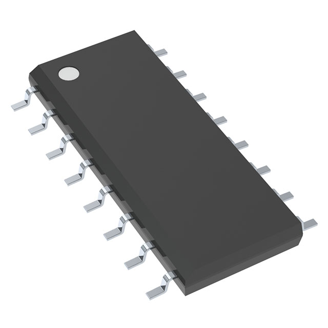
The CD74HC4053M96G3 is a high-performance, 3-channel, single-pole double-throw (SPDT) analog switch designed by Texas Instruments. This IC is part of the 74HC4053 family and is optimized for a wide range of applications requiring reliable switching and multiplexing capabilities. The device is housed in a 16-pin SOIC package, making it suitable for surface-mount applications and ensuring ease of integration into compact electronic designs.
CD74HC4053M96G3 Features
- Low On-State Resistance: The CD74HC4053M96G3 boasts a maximum on-state resistance (R_on) of 130 ohms, ensuring minimal signal attenuation and power loss during switching operations.
- Wide Operating Voltage Range: This IC supports a dual supply voltage range of ±1V to ±5V and a single supply voltage range of 2V to 6V, providing flexibility for various power supply configurations.
- High Channel-to-Channel Matching: With a channel-to-channel matching (ΔR_on) of 5 ohms, the CD74HC4053M96G3 ensures consistent performance across all channels, making it ideal for applications requiring precise signal routing.
- Low Leakage Current: The maximum leakage current (I_S(off)) is rated at 100nA, ensuring minimal power consumption and signal degradation when the switch is in the off state.
- High Bandwidth: The -3dB bandwidth of 200MHz allows the CD74HC4053M96G3 to handle high-frequency signals efficiently, making it suitable for applications in communication and signal processing systems.
- Low Channel Capacitance: The channel capacitance (C_S(off), C_D(off)) is only 8pF, reducing signal distortion and ensuring fast switching times.
- Compliance and Reliability: The CD74HC4053M96G3 is REACH unaffected and RoHS3 compliant, ensuring it meets stringent environmental and safety standards. Additionally, it has a moisture sensitivity level (MSL) of 1, making it suitable for unlimited storage and handling conditions.
CD74HC4053M96G3 Applications
The CD74HC4053M96G3 is ideal for a variety of applications due to its versatile design and robust performance characteristics. Some key applications include:
- Signal Routing and Multiplexing: The 3-channel SPDT switch capability makes this IC perfect for routing multiple signals through a single path, enabling efficient signal management in complex electronic systems.
- Audio and Video Systems: The low on-state resistance and high bandwidth make the CD74HC4053M96G3 suitable for switching audio and video signals without significant loss of signal quality.
- Communication Systems: The high-frequency performance and low capacitance ensure reliable switching of high-speed data signals, making it ideal for use in communication systems and network interfaces.
- Medical and Industrial Equipment: The device's compliance with environmental standards and its high reliability make it suitable for use in medical and industrial applications where precision and safety are critical.
Conclusion of CD74HC4053M96G3
The CD74HC4053M96G3 is a versatile and high-performance analog switch that offers a combination of low on-state resistance, wide operating voltage range, and high bandwidth. Its low leakage current and channel capacitance ensure minimal signal degradation, making it ideal for applications requiring precise signal routing and multiplexing. With its compliance to environmental standards and robust design, the CD74HC4053M96G3 is a reliable choice for a wide range of electronic systems.
Tech Specifications
CD74HC4053M96G3 Documents
Download datasheets and manufacturer documentation for CD74HC4053M96G3
 CDx4HC405x, CDx4HCT405x
  BOM/Assembly Site Updates 03/Dec/2014
  OBS 21/Jun/2023
  CDx4HC405x, CDx4HCT405x
 Shopping Guide


.png?x-oss-process=image/format,webp/resize,h_32)


