
Texas Instruments
CDCLVC1106PWR
Clock Buffers, Drivers ICs


.png?x-oss-process=image/format,webp/resize,p_30)


CDCLVC1106PWR Description
CDCLVC1106PWR Description
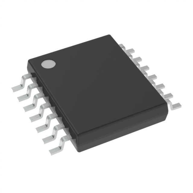
The CDCLVC1106PWR is a high-performance fanout buffer (distribution) IC designed and manufactured by Texas Instruments. This device is specifically engineered for clock buffering applications, offering a 1:6 input-to-output ratio, making it ideal for distributing clock signals across multiple devices or components in a system. With its LVCMOS input and output, the CDCLVC1106PWR ensures compatibility with a wide range of digital systems.
CDCLVC1106PWR Features
-
Technical Specifications:
- ECCN: EAR99
- Input/Output Ratio: 1:6
- Differential Input/Output: No/No
- Mounting Type: Surface Mount
- Voltage - Supply: 2.3V ~ 3.6V
- Output: LVCMOS
- Number of Circuits: 1
- Frequency - Max: 250 MHz
- Moisture Sensitivity Level (MSL): 1 (Unlimited)
-
Performance Benefits:
- High-Speed Operation: Capable of operating at a maximum frequency of 250 MHz, ensuring reliable performance in high-speed digital systems.
- Low Voltage Operation: Compatible with a wide range of supply voltages (2.3V to 3.6V), making it suitable for various power-sensitive applications.
- Surface Mount Technology: Facilitates integration into compact, high-density designs.
-
Compliance and Certifications:
- RoHS Status: ROHS3 Compliant
- REACH Status: REACH Unaffected
-
Packaging: Tape & Reel (TR)
CDCLVC1106PWR Applications
The CDCLVC1106PWR is particularly well-suited for applications where high-speed clock distribution is required. Some specific use cases include:
- High-Speed Data Communication Systems: Ideal for distributing clock signals in high-speed data communication systems, such as Ethernet switches and routers.
- Telecommunications Equipment: Useful in telecommunications equipment where precise clock distribution is critical for signal synchronization.
- Industrial Automation Systems: Employed in industrial automation systems to ensure accurate timing and synchronization of various control components.
- Consumer Electronics: Utilized in consumer electronics, such as gaming consoles and high-definition video playback devices, to maintain precise clock signals across multiple components.
Conclusion of CDCLVC1106PWR
The CDCLVC1106PWR from Texas Instruments stands out as a reliable and high-performance fanout buffer IC, designed to meet the demanding requirements of modern digital systems. Its unique combination of high-speed operation, low voltage compatibility, and surface mount technology makes it an excellent choice for a wide range of applications, from high-speed data communication to consumer electronics. With its compliance with RoHS and REACH regulations, the CDCLVC1106PWR is not only a technically superior product but also an environmentally responsible choice for designers and engineers.
Tech Specifications
CDCLVC1106PWR Documents
Download datasheets and manufacturer documentation for CDCLVC1106PWR
 Mechanical Outline Drawing
  Add Cu as Alternative Bond Wire Metal for Select Devices (PDF) Product Change Notification (PDF)
  CDCLVC1106PWR Symbol & Footprint by SnapMagic
  Clock & Timing Solutions (Rev. C)
  How to Apply 1.8-V Signals to 3.3-V CDCLVC11xx Fanout Clock Buffer
 Shopping Guide


.png?x-oss-process=image/format,webp/resize,h_32)


