
 German
 Japanese
 Portuguese
 Korea
Korea
 Mexico
 Dutch
Dutch


Texas Instruments
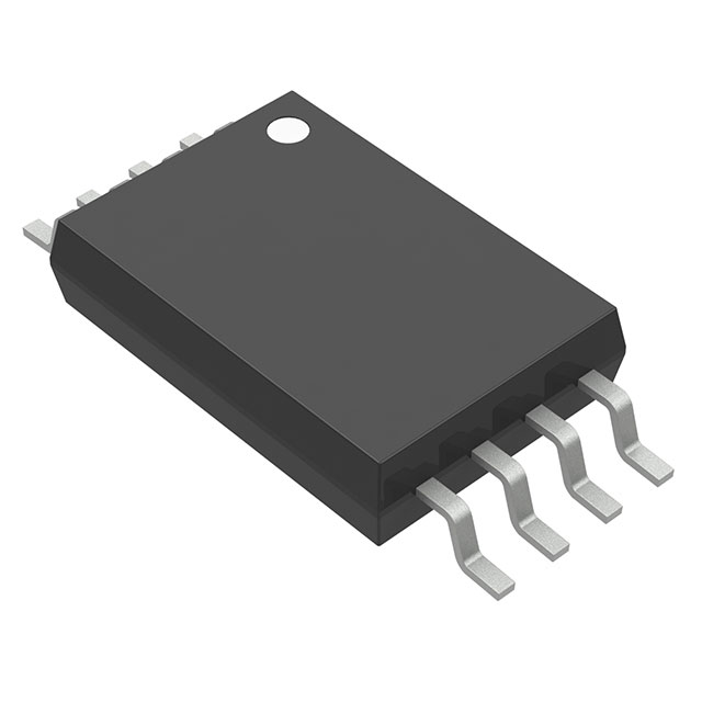
CDCV304PWG4

Why Choose Us?
Professional Platform
B2B & B2C purchasingDelivery at full speed
1-2 days deliveryWide variety
Original manufacturers365 days guarantee
Responsible quality
.png)


Tech Specifications
CDCV304PWG4 Description
CDCV304PWG4 Description
The CDCV304PWG4 is a high-performance clock buffer designed by Texas Instruments, specifically engineered for applications requiring precise clock signal distribution. This device features a 1:4 fanout ratio, allowing it to efficiently distribute a single input clock signal to four output channels. The CDCV304PWG4 operates within a supply voltage range of 2.3V to 3.6V, making it versatile for various power supply configurations. It supports LVTTL input and output levels, ensuring compatibility with a wide range of digital systems. The device is housed in an 8-TSSOP package, which is ideal for surface mount applications, providing robust mechanical stability and ease of integration into compact designs. With a maximum operating frequency of 200 MHz, the CDCV304PWG4 ensures high-speed signal integrity and minimal propagation delay, making it suitable for demanding high-frequency applications.
CDCV304PWG4 Features
- High Fanout Capability: The 1:4 fanout ratio allows the CDCV304PWG4 to distribute a single clock signal across multiple destinations without significant signal degradation.
- Wide Operating Voltage Range: The device operates within a supply voltage range of 2.3V to 3.6V, offering flexibility in power supply design and compatibility with different system architectures.
- High-Speed Performance: With a maximum operating frequency of 200 MHz, the CDCV304PWG4 ensures reliable performance in high-speed clock distribution applications.
- Surface Mount Compatibility: The 8-TSSOP package is designed for surface mount technology, facilitating easy integration into compact and high-density PCB designs.
- LVTTL Compatibility: The device supports LVTTL input and output levels, ensuring seamless integration with other digital components and systems.
- Regulatory Compliance: The CDCV304PWG4 is REACH unaffected and RoHS3 compliant, meeting stringent environmental and safety standards, making it suitable for global deployment.
- Moisture Sensitivity Level: With an MSL of 1 (Unlimited), the device is highly resistant to moisture, ensuring reliability in various environmental conditions.
CDCV304PWG4 Applications
The CDCV304PWG4 is ideal for a variety of applications where precise clock signal distribution is critical. Some specific use cases include:
- Telecommunications: In high-speed communication systems, the CDCV304PWG4 can distribute clock signals to multiple components, ensuring synchronized operation and minimizing timing errors.
- Data Centers: For server farms and data processing units, the device can provide reliable clock distribution to various processing units, maintaining system integrity and performance.
- Consumer Electronics: In devices such as routers, modems, and smart TVs, the CDCV304PWG4 can distribute clock signals to multiple subsystems, ensuring synchronized operation and high performance.
- Industrial Automation: In industrial control systems, the device can distribute clock signals to various sensors and controllers, ensuring precise timing and coordination.
Conclusion of CDCV304PWG4
The CDCV304PWG4 from Texas Instruments is a robust and versatile clock buffer designed to meet the demands of high-speed digital systems. Its 1:4 fanout ratio, wide operating voltage range, and high-frequency performance make it an ideal choice for applications requiring precise clock signal distribution. The device's surface mount compatibility, LVTTL support, and regulatory compliance further enhance its appeal. Whether used in telecommunications, data centers, consumer electronics, or industrial automation, the CDCV304PWG4 offers reliable performance and ease of integration, making it a standout choice in the clock buffer market.
FAQ
Not available to buy online? Want the lower wholesale price? Please Send RFQ to get best price, we will respond immediately


.png?x-oss-process=image/format,webp/resize,h_32)


