Texas Instruments
CDCLVP111VF
Clock Buffers, Drivers ICs


.png?x-oss-process=image/format,webp/resize,p_30)


CDCLVP111VF Description
CDCLVP111VF Description
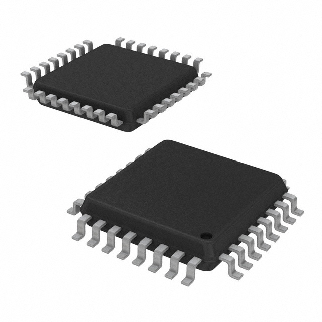
The CDCLVP111VF is a high-performance clock buffer designed by Texas Instruments, specifically tailored for applications requiring precise clock distribution and signal integrity. This device is classified under Clock/Timing ICs and is known for its robust performance and versatility. The CDCLVP111VF features a 2:10 input-to-output ratio, making it ideal for fan-out buffer and multiplexer applications. It supports a wide range of input signal types, including CML, LVDS, LVPECL, and SSTL, ensuring compatibility with various high-speed signaling standards. The output is designed to deliver LVPECL signals, maintaining high fidelity and minimizing jitter.
CDCLVP111VF Features
- Differential Signaling: The CDCLVP111VF supports differential signaling both at the input and output stages, which enhances signal integrity and reduces electromagnetic interference (EMI). This feature is crucial for high-speed applications where signal quality is paramount.
- Wide Supply Voltage Range: The device operates within a supply voltage range of 2.375V to 3.8V, providing flexibility in power supply design and compatibility with different system architectures.
- High-Frequency Performance: With a maximum operating frequency of 3.5 GHz, the CDCLVP111VF is well-suited for high-speed clock distribution and signal routing in demanding applications such as telecommunications, networking, and high-performance computing.
- Surface Mount Technology: The CDCLVP111VF is designed for surface mount applications, offering ease of integration into modern PCB designs and ensuring reliable mechanical and electrical connections.
- Compliance and Reliability: The device is REACH unaffected and RoHS3 compliant, ensuring it meets stringent environmental and safety standards. Additionally, its moisture sensitivity level (MSL) is rated at 1 (unlimited), making it suitable for a wide range of manufacturing environments.
- Packaging and Availability: The CDCLVP111VF is available in a tray package, facilitating efficient handling and storage during manufacturing processes.
CDCLVP111VF Applications
The CDCLVP111VF is designed to meet the demands of various high-speed applications, including:
- Telecommunications: Ideal for clock distribution in base stations and other telecom infrastructure where high-speed, low-jitter clock signals are critical.
- Networking: Suitable for use in routers, switches, and other networking equipment that require reliable clock distribution to maintain data integrity.
- High-Performance Computing: The device's high-frequency capabilities make it a perfect fit for servers and data centers where precise clock synchronization is essential.
- Consumer Electronics: Can be used in high-speed interfaces such as HDMI andPort Display, ensuring high-quality signal transmission.
Conclusion of CDCLVP111VF
The CDCLVP111VF from Texas Instruments stands out as a versatile and high-performance clock buffer, offering a range of features that cater to the needs of modern high-speed applications. Its support for differential signaling, wide supply voltage range, and high-frequency performance make it a reliable choice for clock distribution and signal routing. The device's compliance with environmental and safety standards further enhances its suitability for a wide range of industries. Whether in telecommunications, networking, or high-performance computing, the CDCLVP111VF provides the reliability and performance needed to ensure optimal system operation.
Tech Specifications
CDCLVP111VF Documents
Download datasheets and manufacturer documentation for CDCLVP111VF
 CDCLVP111
  CDCLVP111
 Shopping Guide


.png?x-oss-process=image/format,webp/resize,h_32)


