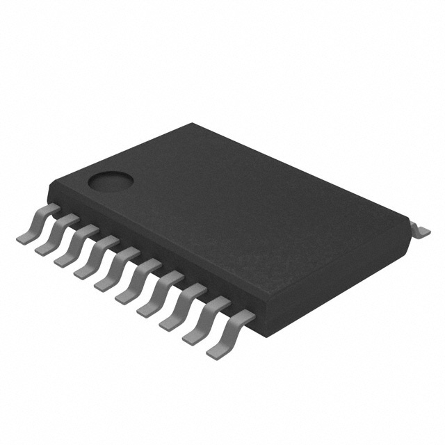
Texas Instruments_CDCLVC1110PW

Texas Instruments
CDCLVC1110PW  
Clock Buffers, Drivers ICs

Texas Instruments
CDCLVC1110PW
764-CDCLVC1110PW
Ersa
Texas Instruments-CDCLVC1110PW-datasheets-7371377.pdf
IC CLK BUF 1:10 250MHZ 20TSSOP
In Stock : 36

Not available to buy online? Want the lower wholesale price? Please Send RFQ to get best price, we will respond immediately

QUICK RFQ
ADD TO RFQ LIST
ersa FreeSample ersa flow
ISO9001
Quality Policy
ISO45001
ISO14001

CDCLVC1110PW Description

This electronic device is available in Tube way. The Tube way of this CDCLVC1110PW save on time, space, energy, and materials. The benefits of this CDCLVC1110PW include low cost, flexibility, reliability, efficiency, and consistency. Texas Instruments produces this CDCLVC1110PW and manage to employ it to various fields. The goals of this Texas Instruments is on the way of becoming one of the best electronic suppliers in Asia-Pacific Region. And it aspires to play a significant role in the growth of the sector. The category level of this CDCLVC1110PW is Clock Buffers, Drivers ICs category. Its highest category level is audio special clock/timing ICs. IC clocks are semiconductor integrated circuits (ICs). IC clocks are important components in virtually all electronic components. They maintain synchronization and timing control in: Telecommunications applications. CDCLVC1110PW offers innovative clock IC and timing IC solutions. It is designed to improve system performance and lower development and manufacturing costs. Products feature low jitter and low phase noise for clock cleanup.

Tech Specifications

Maximum Propagation Delay Time @ Maximum CL (ns)
Fanout
PPAP
Product Status
Automotive
Supplier Package
Input
Package / Case
Absolute Propagation Delay Time (ns)
Voltage - Supply
REACH Status
Maximum Operating Supply Voltage (V)
EU RoHS
Moisture Sensitivity Level (MSL)
Operating Temperature
ECCN
Mounting Type
Standard Package Name
Pin Count
Mounting
Lead Shape
SVHC
Typical Operating Supply Voltage (V)
HTSUS
Package
Input Logic Level
Frequency - Max
PCB changed
HTS
ECCN (US)
Supplier Device Package
Minimum Operating Temperature (°C)
Maximum Operating Temperature (°C)
Output Logic Level
Output
Package Height
Mfr
RoHS Status
Number of Outputs per Chip
Ratio - Input:Output
Differential - Input:Output
Package Length
Series
Type
Part Status
Number of Circuits
Package Width
Base Product Number
Minimum Operating Supply Voltage (V)
Mounting Style
Unit Weight
Input Type
Output Type
Product
RoHS
Supply Voltage - Min
Maximum Input Frequency
Minimum Operating Temperature
Number of Outputs
Propagation Delay - Max
Operating Supply Current
Length
Height
Max Output Freq
Maximum Operating Temperature
Supply Voltage - Max
USHTS
Width

CDCLVC1110PW Documents

Download datasheets and manufacturer documentation for CDCLVC1110PW

Ersa CDCLVC11xx      
Ersa CDCLVC11xx      
Ersa Copper Bond Wire Revision A 04/Dec/2013       Mult PN PART MARKING 08/Dec/2023      

Shopping Guide

Payment Methods
Payment Methods include Prepayment TT (bank transfer), Western Union, and PayPal. Customers are responsible for shipping costs, bank charges, customs duties and taxes.
Shipping Rate
Shipments are made once a day around 5pm, excluding Sundays. Once shipped, the estimated delivery time is usually 5-7 business days, depending on the courier you choose.
Delivery Methods
Provide DHL, FedEx, UPS, EMS, SF Express and Registered Airmail International Delivery Service