
Texas Instruments
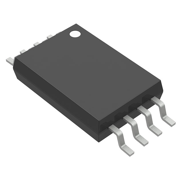
CDCLVC1102PWR
Clock Buffers, Drivers ICs


- 1+
- $1.22710
- $1.23
- 10+
- $1.04825
- $10.48
- 30+
- $0.95054
- $28.52
- 100+
- $0.71705
- $71.7
- 500+
- $0.66737
- $333.69
- 1000+
- $0.64418
- $644.18

.png?x-oss-process=image/format,webp/resize,p_30)


CDCLVC1102PWR Description
The Texas Instruments CDCLVC1102PWR is a high-speed, 2-input OR gate that is designed for use in a wide range of applications. This device is manufactured using CMOS technology, which allows it to operate at high speeds while consuming low power.
Description:
The CDCLVC1102PWR is a 2-input OR gate that is available in a SOIC-8 package. It has a supply voltage range of 2.5V to 5.5V and an operating temperature range of -40°C to +85°C. The device has a propagation delay of 3.5 ns and a typical power consumption of 1.8 mW.
Features:
- High-speed operation: The CDCLVC1102PWR is designed for high-speed applications, with a propagation delay of only 3.5 ns.
- Low power consumption: The device is manufactured using CMOS technology, which allows it to operate at low power levels.
- Wide supply voltage range: The CDCLVC1102PWR can operate with a supply voltage range of 2.5V to 5.5V, making it suitable for a variety of applications.
- Wide operating temperature range: The device can operate in a wide range of temperatures, from -40°C to +85°C.
- 2-input OR gate: The CDCLVC1102PWR is a 2-input OR gate, which means that the output will be high if either of the inputs is high.
Applications:
The CDCLVC1102PWR is suitable for a wide range of applications, including:
- Digital circuits: The device can be used in digital circuits to perform logical OR operations.
- High-speed data transmission: The high-speed operation of the CDCLVC1102PWR makes it suitable for use in high-speed data transmission applications.
- Power management: The low power consumption of the device makes it suitable for use in power management applications.
- Industrial control systems: The wide operating temperature range of the CDCLVC1102PWR makes it suitable for use in industrial control systems.
Overall, the Texas Instruments CDCLVC1102PWR is a high-speed, low-power, 2-input OR gate that is suitable for a wide range of applications. Its high-speed operation, low power consumption, and wide operating temperature range make it an ideal choice for digital circuits, high-speed data transmission, power management, and industrial control systems.
Tech Specifications
CDCLVC1102PWR Documents
Download datasheets and manufacturer documentation for CDCLVC1102PWR
 CDCLVC11xx
  CDCLVC11xx
  Copper Bond Wire Revision A 04/Dec/2013 Design 22/Feb/2022
 Shopping Guide


.png?x-oss-process=image/format,webp/resize,h_32)


