
 German
 Japanese
 Portuguese
 Korea
Korea
 Mexico
 Dutch
Dutch


Texas Instruments
CLV4051ATDWRG4Q1

Why Choose Us?
Professional Platform
B2B & B2C purchasingDelivery at full speed
1-2 days deliveryWide variety
Original manufacturers365 days guarantee
Responsible quality
.png)


Tech Specifications
CLV4051ATDWRG4Q1 Description
CLV4051ATDWRG4Q1 Description
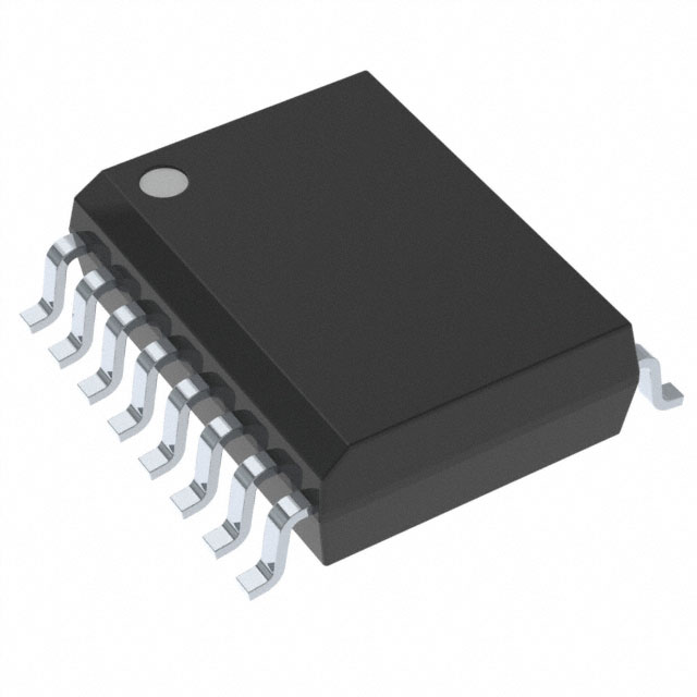
The CLV4051ATDWRG4Q1 is a high-performance 8:1 multiplexer/demultiplexer integrated circuit designed for demanding automotive applications. Manufactured by Texas Instruments, this device offers a robust combination of low on-state resistance, fast switching times, and excellent channel matching, making it ideal for a variety of signal routing and conditioning tasks. The CLV4051ATDWRG4Q1 is housed in a surface-mount 16SOIC package, ensuring ease of integration into compact and high-density designs. With a supply voltage range of 2V to 5.5V, it provides flexibility for various power supply configurations.
CLV4051ATDWRG4Q1 Features
- Low On-State Resistance: The maximum on-state resistance of 75Ω ensures minimal signal attenuation and power loss, making it suitable for applications requiring high signal integrity.
- Fast Switching Times: With a switch time of 14ns for both turn-on and turn-off, the CLV4051ATDWRG4Q1 can handle high-speed signals efficiently, reducing latency and improving overall system performance.
- Channel-to-Channel Matching: The 1.3Ω channel-to-channel matching ensures consistent performance across all channels, which is crucial for applications requiring precise signal routing.
- Low Leakage Current: The maximum leakage current of 100nA minimizes power consumption and signal degradation, enhancing the reliability and efficiency of the circuit.
- Wide Bandwidth: The -3dB bandwidth of 35MHz supports a wide range of signal frequencies, making it suitable for both analog and digital signal processing.
- Compliance and Reliability: The CLV4051ATDWRG4Q1 is REACH unaffected and RoHS3 compliant, ensuring environmental sustainability and regulatory compliance. Additionally, its moisture sensitivity level (MSL) of 1 (unlimited) guarantees high reliability in various environmental conditions.
- Automotive Grade: Designed for automotive applications, the CLV4051ATDWRG4Q1 meets the stringent requirements of the automotive industry, ensuring robust performance and durability.
CLV4051ATDWRG4Q1 Applications
The CLV4051ATDWRG4Q1 is well-suited for a variety of applications, particularly in the automotive sector, where its high performance and reliability are critical. Some specific use cases include:
- Automotive Signal Routing: Ideal for routing signals in automotive electronic control units (ECUs), infotainment systems, and advanced driver-assistance systems (ADAS).
- High-Speed Data Communication: Suitable for applications requiring fast and reliable data transmission, such as automotive Ethernet and other high-speed communication protocols.
- Signal Conditioning: Can be used in signal conditioning circuits to route and process analog and digital signals with minimal distortion.
- Multiplexing and Demultiplexing: Efficiently handles the multiplexing and demultiplexing of multiple signals, reducing the number of required channels and simplifying circuit design.
Conclusion of CLV4051ATDWRG4Q1
The CLV4051ATDWRG4Q1 from Texas Instruments is a versatile and high-performance 8:1 multiplexer/demultiplexer IC designed to meet the demanding requirements of automotive applications. Its low on-state resistance, fast switching times, and excellent channel matching make it an ideal choice for signal routing and conditioning tasks. The device's compliance with industry standards and its automotive grade ensure reliability and durability in harsh environments. Whether used in automotive ECUs, infotainment systems, or high-speed data communication, the CLV4051ATDWRG4Q1 offers a reliable and efficient solution for signal management.
FAQ
| Quantity | Unit Price | Ext. Price |
|---|---|---|
| 1+ | $0.59840 | $0.60 |
| 10+ | $0.42328 | $4.23 |
| 25+ | $0.38016 | $9.50 |
| 100+ | $0.33229 | $33.23 |
| 250+ | $0.30951 | $77.38 |
Not available to buy online? Want the lower wholesale price? Please Send RFQ to get best price, we will respond immediately


.png?x-oss-process=image/format,webp/resize,h_32)


