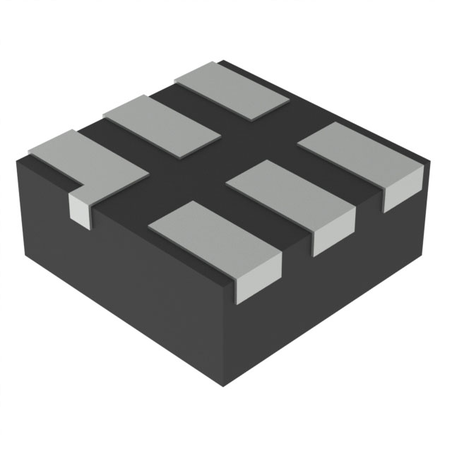
Texas Instruments_SN74LVC1G3157DTBR

Texas Instruments
SN74LVC1G3157DTBR  
Analog Switches, Multiplexers, Demultiplexers

Texas Instruments
SN74LVC1G3157DTBR
747-SN74LVC1G3157DTBR
Ersa
Texas Instruments-SN74LVC1G3157DTBR-datasheets-277407.pdf
IC SWITCH SPDT X 1 15OHM 6X2SON
In Stock : 6888

Not available to buy online? Want the lower wholesale price? Please Send RFQ to get best price, we will respond immediately

QUICK RFQ
ADD TO RFQ LIST
ersa FreeSample ersa flow
ISO9001
Quality Policy
ISO45001
ISO14001

SN74LVC1G3157DTBR Description

The SN74LVC1G3157DTBR is a high-performance, single 2-to-1 multiplexer (MUX) manufactured by Texas Instruments. It is part of the 74LVC1G3157 series, which is designed to provide low-power consumption and high noise immunity in a compact package. Here's a brief description, features, and applications of the SN74LVC1G3157DTBR:

Description:

The SN74LVC1G3157DTBR is a logic device that allows the selection of one of two input signals to be passed to a single output. It is designed to operate with low voltage supplies and has a low on-chip power dissipation, making it suitable for battery-powered and portable applications.

Features:

  1. Single 2-to-1 multiplexer function
  2. Low-power consumption: 1.65 mA maximum at a supply voltage of 1.65V to 3.6V
  3. High noise immunity: 10 kV/µs (typical) propagation delay variation
  4. Wide operating voltage range: 1.65V to 3.6V
  5. Low on-chip power dissipation
  6. Available in a small SOT-23 package
  7. RoHS-compliant and lead-free

Applications:

  1. Digital signal processing systems
  2. Battery-powered and portable devices
  3. Telecommunication equipment
  4. Industrial control systems
  5. Automotive electronics
  6. Consumer electronics
  7. Microcontroller-based systems

The SN74LVC1G3157DTBR is a versatile and efficient multiplexer that can be used in various applications where signal selection is required. Its low-power consumption and high noise immunity make it an excellent choice for applications that demand energy efficiency and reliable performance.

Tech Specifications

Number of Channels per Chip
Unit Weight
Power Supply Type
Protocols
Configuration
Crosstalk
Input/output continuous current (max) (mA)
PPAP
Voltage - Supply, Dual (V±)
Automotive
RoHS
Maximum High Level Output Current (mA)
Channel Capacitance (CS(off), CD(off))
On-State Resistance (Max)
REACH Status
Multiplexer/Demultiplexer Circuit
Switch Time (Ton, Toff) (Max)
Operating temperature range (°C)
Standard Package Name
Maximum On Resistance Range (Ohm)
Mounting
Input Signal Type
Minimum Single Supply Voltage (V)
Supply current (typ) (µA)
Package
Switch Architecture
Current - Leakage (IS(off)) (Max)
Off Time - Max
Minimum Dual Supply Voltage
Supply Current - Max
Channel-to-Channel Matching (ΔRon)
Package Height
Charge Injection
Maximum Operating Temperature
Bandwidth (MHz)
RoHS Status
Number of channels
Switch Continuous Current
Number of Inputs per Chip
-3db Bandwidth
Maximum Low Level Output Current (mA)
Minimum Operating Temperature
Voltage - Supply, Single (V+)
Type
Ron (typ) (Ω)
Switch Circuit
Part Status
Supply Type
Lead finish / Ball material
Number of Circuits
Package Width
CON (typ) (pF)
Output Signal Type
Maximum Turn-On Time (ns)
Product Status
Supplier Package
Package / Case
Number of Channels
EU RoHS
Carrier
Maximum Turn-Off Time (ns)
Moisture Sensitivity Level (MSL)
Operating Temperature
Maximum Frequency (25°C) @ Vcc (MHz)
ECCN
On Resistance - Max
MSL rating / Peak reflow
Mounting Type
Pin Count
Drain supply voltage (max) (V)
Lead Shape
HTSUS
Pins
USHTS
ON-state leakage current (max) (µA)
On Time - Max
Maximum Dual Supply Voltage
PCB changed
HTS
Rating
ECCN (US)
Power supply voltage - single (V)
Supplier Device Package
Supply Voltage - Min
Minimum Operating Temperature (°C)
Maximum Operating Temperature (°C)
Mfr
Polarity
Supply voltage (max) (V)
Features
Supply Voltage - Max
Maximum On Resistance (Ohm)
Mounting Style
Typical Single Supply Voltage (V)
Maximum Propagation Delay Bus to Bus (ns)
Number of Outputs per Chip
Chip Enable Signals
Package Length
Maximum Supply Current (mA)
REACH
Series
Maximum Single Supply Voltage (V)
Base Product Number

SN74LVC1G3157DTBR Documents

Download datasheets and manufacturer documentation for SN74LVC1G3157DTBR

Ersa SN74LVC1G3157 Datasheet       Logic Guide      
Ersa Signal Switch Data Book      
Ersa SN74LVC1G3157 Datasheet       Logic Guide      
Ersa SN74LVC1G3157 22/Aug/2022      

Shopping Guide

Payment Methods
Payment Methods include Prepayment TT (bank transfer), Western Union, and PayPal. Customers are responsible for shipping costs, bank charges, customs duties and taxes.
Shipping Rate
Shipments are made once a day around 5pm, excluding Sundays. Once shipped, the estimated delivery time is usually 5-7 business days, depending on the courier you choose.
Delivery Methods
Provide DHL, FedEx, UPS, EMS, SF Express and Registered Airmail International Delivery Service