

Texas Instruments
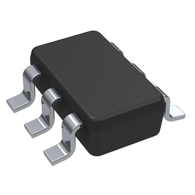
INA181A3QDBVRQ1
OP Amps, Buffer Amps ICs

Not available to buy online? Want the lower wholesale price? Please Send RFQ to get best price, we will respond immediately


- 1+
- $0.55476
- $0.55
- 10+
- $0.45043
- $4.5
- 30+
- $0.39910
- $11.97
- 100+
- $0.34610
- $34.61

.png?x-oss-process=image/format,webp/resize,p_30)


INA181A3QDBVRQ1 Description
The INA181A3QDBVRQ1 is a high-precision, low-power, monolithic current shunt amplifier designed for use in battery monitoring and management systems. It is manufactured by Texas Instruments, a leading semiconductor company known for its high-quality electronic components.
Description:
The INA181A3QDBVRQ1 is a precision current shunt amplifier that can be used to measure both positive and negative currents. It is available in a compact, thermally enhanced, 16-lead QFN package. The device features a high common-mode voltage range, which allows it to operate in harsh environments and with high-side or low-side shunt resistors.
Features:
- High precision: The INA181A3QDBVRQ1 offers high accuracy and low drift, making it suitable for a wide range of applications.
- Low power consumption: The device operates with a low supply current, making it ideal for battery-powered systems.
- Wide input voltage range: The INA181A3QDBVRQ1 can operate with input voltages from 2.7V to 5.5V, making it suitable for a variety of power supply configurations.
- High common-mode voltage range: The device can operate with a common-mode voltage range of up to ±70V, allowing it to work with high-side or low-side shunt resistors.
- Programmable gain: The gain of the INA181A3QDBVRQ1 can be programmed using an external resistor, allowing for customization of the output current range.
- Wide temperature range: The device is specified to operate over a wide temperature range of -40°C to +125°C, making it suitable for use in harsh environments.
Applications:
- Battery monitoring systems: The INA181A3QDBVRQ1 is ideal for use in battery monitoring systems, where it can be used to measure the current flowing in and out of the battery.
- Energy harvesting systems: The device can be used in energy harvesting systems to measure the current generated by renewable energy sources such as solar panels or wind turbines.
- Electric vehicle (EV) battery management systems: The INA181A3QDBVRQ1 can be used in EV battery management systems to monitor the current flowing in and out of the battery, helping to ensure safe and efficient operation.
- Power supply monitoring: The device can be used to monitor the current flowing in and out of power supplies, helping to ensure that they are operating within their specified limits.
- Industrial control systems: The INA181A3QDBVRQ1 can be used in industrial control systems to measure the current flowing through various components, helping to ensure that they are operating correctly and efficiently.
In summary, the INA181A3QDBVRQ1 is a high-precision, low-power current shunt amplifier that offers a wide range of features and is suitable for a variety of applications, including battery monitoring systems, energy harvesting systems, electric vehicle battery management systems, power supply monitoring, and industrial control systems.
Tech Specifications
INA181A3QDBVRQ1 Documents
Download datasheets and manufacturer documentation for INA181A3QDBVRQ1
Assembly Material 05/Jun/2023 INA181-Q1, INA2181-Q1, INA4181-Q1 Symbolization Change 04/Nov/2020 INA181-Q1, INA2181-Q1, INA4181-Q1 Related Parts


Shopping Guide


.png?x-oss-process=image/format,webp/resize,h_32)


©2025 ERSA Electronics Corporation.