
 German
 Japanese
 Portuguese
 Korea
Korea
 Mexico
 Dutch
Dutch


Texas Instruments
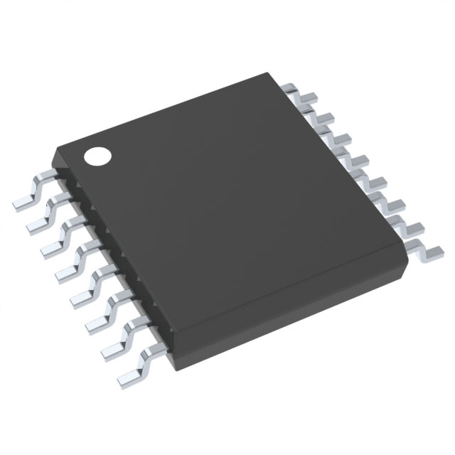
SN74LV4053APW

Why Choose Us?
Professional Platform
B2B & B2C purchasingDelivery at full speed
1-2 days deliveryWide variety
Original manufacturers365 days guarantee
Responsible quality
.png)


Tech Specifications
SN74LV4053APW Description
SN74LV4053APW Description
The SN74LV4053APW from Texas Instruments is a high-performance triple SPDT (Single-Pole Double-Throw) analog switch/multiplexer-demultiplexer IC, designed for low-voltage digital and analog signal routing. Housed in a 16-pin TSSOP package, it features three independent 2:1 multiplexer/demultiplexer circuits, making it ideal for signal gating, routing, and switching applications. With an ultra-low leakage current of 100nA (max) and low on-state resistance (75Ω max), it ensures minimal signal distortion and power loss. The device operates over a wide supply voltage range (2V to 5.5V), supporting compatibility with both 3.3V and 5V systems. Its 50MHz bandwidth and fast switching times (14ns Ton/Toff) make it suitable for high-speed signal processing.
SN74LV4053APW Features
- Low On-Resistance (75Ω max) ensures minimal signal attenuation.
- Low Leakage Current (100nA max) for high signal integrity in precision applications.
- Fast Switching (14ns Ton/Toff) enables high-speed signal routing.
- Wide Supply Range (2V–5.5V) supports mixed-voltage systems.
- Low Channel Capacitance (0.5pF CS(off), 8.2pF CD(off)) reduces crosstalk and improves bandwidth.
- Matched Channel Resistance (ΔRon 1.3Ω) for consistent signal performance.
- 3 Independent SPDT Switches for flexible signal routing.
- RoHS3 Compliant & REACH Unaffected, meeting environmental standards.
- Surface-Mount TSSOP-16 Package for compact PCB designs.
SN74LV4053APW Applications
- Audio/Video Signal Routing: Ideal for AV switches, HDMI multiplexers, and audio crosspoint switches.
- Data Acquisition Systems: Used in ADC/DAC signal conditioning and multiplexing.
- Battery-Powered Devices: Low leakage and wide voltage range suit portable electronics.
- Test & Measurement Equipment: High bandwidth and fast switching support precision instrumentation.
- Communication Systems: Signal routing in RF and baseband applications.
- Industrial Control: Reliable switching for PLCs and sensor interfaces.
Conclusion of SN74LV4053APW
The SN74LV4053APW stands out for its low on-resistance, fast switching, and wide voltage compatibility, making it a versatile solution for analog and digital signal routing. Its low power consumption and high bandwidth are particularly beneficial for portable, high-speed, and precision applications. While marked as Last Time Buy, its performance and reliability ensure it remains a preferred choice for designers needing robust signal switching in space-constrained designs.
FAQ
| Quantity | Unit Price | Ext. Price |
|---|---|---|
| 1+ | $0.94160 | $0.94 |
| 10+ | $0.67936 | $6.79 |
| 90+ | $0.54629 | $49.17 |
| 180+ | $0.51857 | $93.34 |
| 321+ | $0.81840 | $262.71 |
Not available to buy online? Want the lower wholesale price? Please Send RFQ to get best price, we will respond immediately


.png?x-oss-process=image/format,webp/resize,h_32)


