
 German
 Japanese
 Portuguese
 Korea
Korea
 Mexico
 Dutch
Dutch


Texas Instruments
THS3201DGN

Why Choose Us?
Professional Platform
B2B & B2C purchasingDelivery at full speed
1-2 days deliveryWide variety
Original manufacturers365 days guarantee
Responsible quality
.png)


Tech Specifications
THS3201DGN Description
THS3201DGN Description
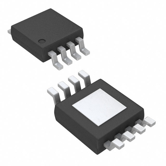
The THS3201DGN is a high-performance current feedback operational amplifier (op-amp) from Texas Instruments, designed for demanding applications requiring high bandwidth and exceptional slew rate. This single-channel amplifier features a wide supply voltage range from 6.6 V to 15 V, making it suitable for various power supply configurations. The THS3201DGN is housed in an 8-pin high voltage small outline package (HVSSOP), which is ideal for surface-mount applications and ensures robust mechanical stability.
THS3201DGN Features
- High Bandwidth and Slew Rate: The THS3201DGN boasts a -3 dB bandwidth of 1.8 GHz and an impressive slew rate of 9800 V/µs. These characteristics make it ideal for high-frequency applications where rapid signal transitions are critical.
- Low Input Bias Current: With an input bias current of 14 µA, the THS3201DGN ensures minimal loading on the signal source, preserving integrity signal.
- Low Input Offset Voltage: The input offset voltage of 700 µV ensures high accuracy in signal processing, making it suitable for precision applications.
- High Output Current: The amplifier can deliver up to 115 mA per channel, enabling it to drive demanding loads effectively.
- Compliance and Packaging: The THS3201DGN is REACH unaffected and RoHS3 compliant, ensuring it meets stringent environmental and regulatory standards. It is also packaged in a tube, which facilitates easy handling and storage.
- Moisture Sensitivity Level: With an MSL rating of 1 (unlimited), the THS3201DGN is suitable for use in various environmental conditions without the need for special handling procedures.
THS3201DGN Applications
The THS3201DGN is well-suited for a variety of high-frequency and high-speed applications, including:
- RF and Microwave Systems: Its high bandwidth and slew rate make it ideal for amplifying and processing high-frequency signals in communication systems.
- High Data-Speed Converters: The amplifier can interface with analog-to-digital converters (ADCs) and digital-to-analog converters (DACs) to ensure high-speed signal processing.
- Video Signal Processing: The THS3201DGN can be used in video signal chains to amplify and process video signals with minimal distortion.
- Pulse Processing: Its high slew rate and low input offset voltage make it suitable for applications involving fast-rising and falling pulses, such as in radar and medical imaging systems.
Conclusion of THS3201D
GNThe THS3201DGN from Texas Instruments is a versatile and high-performance current feedback operational amplifier designed for high-frequency and high-speed applications. Its wide supply voltage range, high bandwidth, and exceptional slew rate make it a standout choice for demanding applications. The low input bias current and input offset voltage ensure high accuracy and minimal signal distortion. While it is marked as "Not For New Designs," the THS3201DGN remains a reliable option for existing designs and applications where its unique features and performance benefits are required.
FAQ
Not available to buy online? Want the lower wholesale price? Please Send RFQ to get best price, we will respond immediately


.png?x-oss-process=image/format,webp/resize,h_32)


