
 German
 Japanese
 Portuguese
 Korea
Korea
 Mexico
 Dutch
Dutch


Texas Instruments
CDCF5801DBQ

Why Choose Us?
Professional Platform
B2B & B2C purchasingDelivery at full speed
1-2 days deliveryWide variety
Original manufacturers365 days guarantee
Responsible quality
.png)


Tech Specifications
CDCF5801DBQ Description
CDCF5801DBQ Description
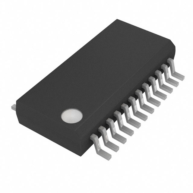
The CDCF5801DBQ is a high-performance PLL (Phase-Locked Loop) multiplier/divider IC designed by Texas Instruments. This device is specifically tailored for applications requiring precise clock generation and frequency manipulation. It features a wide operating voltage range of 3V to 3.6V and supports multiple input and output signal standards, including HSTL, LVPECL, LVTTL, LVDS, and SSTL. The CDCF5801DBQ is housed in a 24-pin surface-mount package, making it suitable for compact and high-density PCB designs.
CDCF5801DBQ Features
- PLL Technology: The CDCF5801DBQ incorporates a robust PLL that ensures stable and accurate frequency multiplication and division. This feature is crucial for maintaining signal integrity and minimizing jitter in high-speed digital systems.
- Wide Input and Output Compatibility: The device supports a variety of input and output signal standards, providing flexibility in system design. This versatility allows it to interface seamlessly with different types of digital circuits.
- Frequency Range: With a maximum operating frequency of 280MHz, the CDCF5801DBQ is well-suited for high-speed applications. This high-frequency capability ensures that it can meet the demands of modern digital systems.
- Compliance and Reliability: The CDCF5801DBQ is REACH unaffected and RoHS3 compliant, ensuring that it meets stringent environmental and safety standards. Additionally, it has a moisture sensitivity level (MSL) of 2, which guarantees reliability in various environmental conditions.
- Package and Mounting: The 24SSOP package and surface-mount mounting type make the CDCF5801DBQ ideal for space-constrained designs. This packaging option also facilitates automated assembly processes, enhancing manufacturing efficiency.
CDCF5801DBQ Applications
The CDCF5801DBQ is ideal for a range of applications where precise clock generation and frequency manipulation are essential. Some specific use cases include:
- High-Speed Communication Systems: In systems requiring high-frequency clock signals, the CDCF5801DBQ can generate and distribute accurate clock signals, ensuring reliable data transmission.
- Digital Signal Processing (DSP): The device's ability to manipulate clock frequencies makes it suitable for DSP applications, where precise timing is critical for signal processing tasks.
- FPGA and ASIC Clocking: The CDCF5801DBQ can be used to generate clock signals for FPGAs and ASICs, providing the necessary timing references for these complex digital devices.
- Test and Measurement Equipment: In precision measurement applications, the CDCF5801DBQ can generate stable and accurate clock signals, enhancing the accuracy and reliability of test equipment.
Conclusion of CDCF5801DBQ
The CDCF5801DBQ from Texas Instruments is a versatile and high-performance PLL multiplier/divider IC. Its wide range of input and output signal standards, combined with its high-frequency capability and robust PLL technology, make it an excellent choice for a variety of high-speed digital applications. The device's compliance with environmental and safety standards, along with its compact surface-mount package, further enhance its appeal for modern electronics designs. While it is marked as "Not For New Designs," the CDCF5801DBQ remains a reliable option for existing systems and applications requiring precise clock generation and frequency manipulation.
FAQ
Not available to buy online? Want the lower wholesale price? Please Send RFQ to get best price, we will respond immediately


.png?x-oss-process=image/format,webp/resize,h_32)


