
Texas Instruments
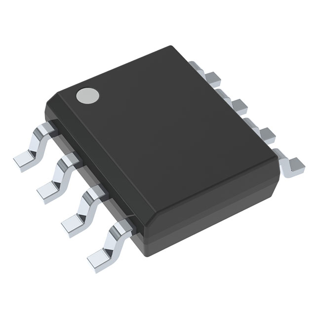
THS4062CD
OP Amps, Buffer Amps ICs


.png?x-oss-process=image/format,webp/resize,p_30)


THS4062CD Description
THS4062CD Description
The THS4062CD from Texas Instruments is a high-performance dual-channel voltage feedback operational amplifier designed for precision applications requiring wide bandwidth and fast signal processing. Packaged in an 8-SOIC tube, this ROHS3 Compliant and REACH Unaffected device operates over a 9V to 32V supply range, making it versatile for both industrial and consumer electronics. With a 180 MHz bandwidth, 400V/µs slew rate, and 115 mA output current per channel, it excels in high-speed signal conditioning, active filtering, and data acquisition systems. Its low input bias current (3 µA) and moderate offset voltage (2.5 mV) ensure accuracy in sensitive analog circuits.
THS4062CD Features
- Wide Supply Range: 9V–32V operation for flexible power supply configurations.
- High-Speed Performance: 180 MHz bandwidth and 400V/µs slew rate enable rapid signal processing.
- Dual-Channel Design: Two independent amplifiers in a compact 8-SOIC package.
- Robust Output Drive: 115 mA/channel current output for driving capacitive or low-impedance loads.
- Low Power Consumption: 7.8 mA per channel supply current balances performance and efficiency.
- Industrial Temperature Range: Operates reliably from 0°C to 70°C, suitable for harsh environments.
THS4062CD Applications
- High-Speed Data Acquisition: Ideal for ADC/DAC buffer stages due to its wide bandwidth and low distortion.
- Active Filters & Equalizers: The high slew rate ensures minimal phase distortion in RF and audio systems.
- Test & Measurement Equipment: Precision signal amplification in oscilloscopes and spectrum analyzers.
- Medical Imaging Systems: Fast response and stability make it suitable for ultrasound and MRI signal chains.
- Industrial Automation: Used in servo control and sensor interfaces requiring high-speed feedback loops.
Conclusion of THS4062CD
The THS4062CD stands out as a high-speed, dual-channel op-amp with exceptional bandwidth and drive capability, making it a top choice for demanding analog applications. Its wide supply range, low noise, and robust performance cater to industries ranging from medical to industrial automation. Engineers will appreciate its balance of speed, precision, and power efficiency, ensuring reliable operation in high-performance systems. For designs requiring fast signal processing with minimal distortion, this amplifier delivers superior results.
Tech Specifications
THS4062CD Documents
Download datasheets and manufacturer documentation for THS4062CD
 THS4062IDR
  THS4062IDR
  Design 25/Feb/2022
 Shopping Guide


.png?x-oss-process=image/format,webp/resize,h_32)


