
Texas Instruments
TLC2252ID
OP Amps, Buffer Amps ICs


.png?x-oss-process=image/format,webp/resize,p_30)


TLC2252ID Description
TLC2252ID Description
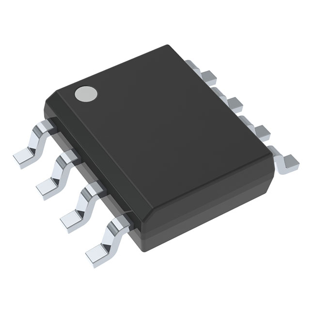
The TLC2252ID is a general-purpose operational amplifier from Texas Instruments, designed for a wide range of applications requiring reliable and efficient signal processing. This dual-channel op-amp features a supply voltage range from 4.4 V to 16 V, making it suitable for both low-power and higher voltage applications. The TLC2252ID offers a gain bandwidth product of 210 kHz, ensuring stable performance across various frequencies. Its low input bias current of 1 pA and input offset voltage of 200 µV make it ideal for precision signal conditioning tasks. The device is housed in a surface-mount 8SOIC package, providing a compact and robust solution for space-constrained designs.
TLC2252ID Features
- Supply Voltage Range: The TLC2252ID operates over a wide supply voltage range of 4.4 V to 16 V, offering flexibility in power supply requirements.
- Gain Bandwidth Product: With a gain bandwidth product of 210 kHz, this op-amp ensures stable performance across a broad frequency spectrum, making it suitable for various analog signal processing applications.
- Low Input Bias Current: The extremely low input bias current of 1 pA minimizes the loading effect on high-impedance sources, ensuring accurate signal amplification.
- Low Input Offset Voltage: The low input offset voltage of 200 µV enhances the accuracy of the amplified signal, making it ideal for precision applications.
- Slew Rate: The slew rate of 0.12 V/µs ensures a smooth and accurate response to rapidly changing input signals.
- Supply Current: The low supply current of 80 µA per channel (160 µA total) makes the TLC2252ID highly energy-efficient, reducing power consumption in battery-operated and low-power systems.
- Output Current: Each channel can deliver up to 50 mA of output current, providing sufficient drive capability for various loads.
- Package: The surface-mount 8SOIC package offers a compact and robust solution, suitable for space-constrained designs and automated assembly processes.
- Compliance and Status: The TLC2252ID is REACH unaffected and RoHS3 compliant, ensuring it meets environmental and regulatory standards. It is also classified under ECCN EAR99 and HTSUS 8542.33.0001, facilitating international trade and compliance.
TLC2252ID Applications
The TLC2252ID is well-suited for a variety of applications where precision and low power consumption are critical. Some specific use cases include:
- Signal Conditioning: Ideal for amplifying and conditioning low-level signals from sensors, ensuring accurate and reliable data acquisition.
- Battery-Powered Devices: Its low power consumption makes it suitable for portable and battery-operated equipment, extending operational time without compromising performance.
- Industrial Control Systems: The wide supply voltage range and robust performance make it suitable for industrial applications where reliability and precision are paramount.
- Medical Equipment: The low input bias current and offset voltage ensure accurate signal processing in medical devices, contributing to precise diagnostics and monitoring.
- Consumer Electronics: The TLC2252ID can be used in consumer electronics for audio signal processing, ensuring high-quality sound reproduction.
Conclusion of TLC2252ID
The TLC2252ID is a versatile and reliable general-purpose operational amplifier from Texas Instruments, offering a wide range of features that make it suitable for various applications. Its low power consumption, wide supply voltage range, and precision performance make it an excellent choice for designers looking for a compact and efficient solution. Despite being marked as obsolete, the TLC2252ID remains a valuable component for applications where its unique features and performance benefits are required.
Tech Specifications
TLC2252ID Documents
Download datasheets and manufacturer documentation for TLC2252ID
 Product Discontinuance Notification (PDF)
  Mechanical Outline Drawing
  Qualification of Alternate Material Set for Assembly with Au Wire and Cu as Additional Wire Base Metal Option for Select SOIC Package Devices (PDF)
  TLC2252ID Symbol & Footprint by SnapMagic
  TLC2252 TINA-TI Reference Design TLC2252 TINA-TI Reference Design (Rev. A)
  TLC2252, TLC2252A PSpice Model (Rev. B) TLC2252, TLC2252A PSpice Model (Rev. A) TLC2252 TINA-TI Spice Model (Rev. A) TLC2252 TINA-TI Spice Model TLC2252, TLC2252A PSpice Model
 Shopping Guide


.png?x-oss-process=image/format,webp/resize,h_32)


