
 German
 Japanese
 Portuguese
 Korea
Korea
 Mexico
 Dutch
Dutch


Texas Instruments
TLC2262AIPW

Why Choose Us?
Professional Platform
B2B & B2C purchasingDelivery at full speed
1-2 days deliveryWide variety
Original manufacturers365 days guarantee
Responsible quality
.png)


Tech Specifications
TLC2262AIPW Description
TLC2262AIPW Description
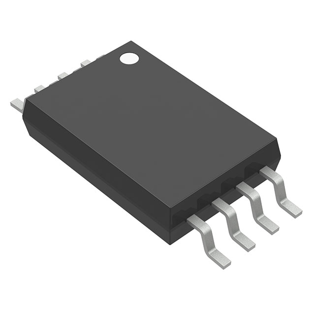
The TLC2262AIPW from Texas Instruments is a dual-channel CMOS operational amplifier belonging to the LinCMOS™ series. Designed for precision low-power applications, it operates within a supply voltage range of 4.4V to 16V, making it suitable for both single and dual-supply configurations. With an ultra-low input bias current of 1 pA and a gain bandwidth product of 730 kHz, this IC delivers high accuracy and stable performance in signal conditioning and amplification tasks. The TLC2262AIPW is housed in an 8-pin TSSOP package, optimized for surface-mount designs, and is RoHS3 compliant with REACH unaffected status.
TLC2262AIPW Features
- Low Power Consumption: 425µA per channel supply current, ideal for battery-operated devices.
- High Precision: 300 µV input offset voltage ensures minimal error in sensitive applications.
- Robust Output Drive: 50 mA output current per channel supports moderate load requirements.
- CMOS Technology: Delivers rail-to-rail output swing and low noise for precision analog circuits.
- Wide Supply Range: 4.4V–16V operation accommodates diverse power sources.
- Slew Rate: 0.55V/µs balances speed and power efficiency for general-purpose use.
TLC2262AIPW Applications
- Portable Instrumentation: Ideal for handheld meters and sensors due to low power and high accuracy.
- Signal Conditioning: Suitable for filtering, buffering, and amplification in data acquisition systems.
- Medical Devices: Used in low-power, high-impedance circuits like ECG amplifiers.
- Industrial Controls: Reliable performance in process monitoring and automation systems.
- Consumer Electronics: Audio preamps, sensor interfaces, and battery management circuits.
Conclusion of TLC2262AIPW
The TLC2262AIPW excels in low-power, precision applications where high input impedance and moderate bandwidth are critical. Its CMOS architecture and wide voltage range make it versatile for portable and industrial designs. While marked obsolete, it remains a dependable choice for legacy systems or designs requiring its specific performance profile. Engineers should evaluate alternatives for new designs but can leverage this IC’s strengths in existing applications.
FAQ
Not available to buy online? Want the lower wholesale price? Please Send RFQ to get best price, we will respond immediately


.png?x-oss-process=image/format,webp/resize,h_32)


