
 German
 Japanese
 Portuguese
 Korea
Korea
 Mexico
 Dutch
Dutch


Texas Instruments
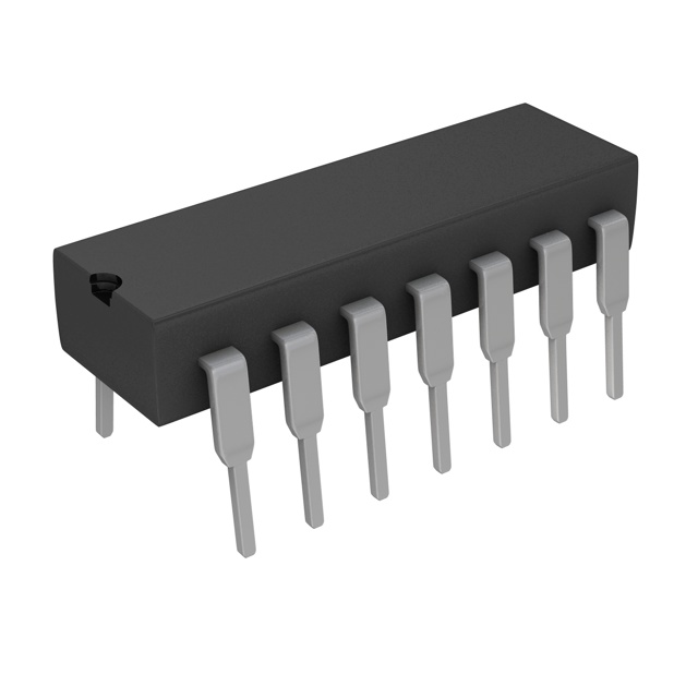
TLC279IN

Why Choose Us?
Professional Platform
B2B & B2C purchasingDelivery at full speed
1-2 days deliveryWide variety
Original manufacturers365 days guarantee
Responsible quality
.png)


Tech Specifications
TLC279IN Description
TLC279IN Description
The TLC279IN is a high-performance CMOS operational amplifier from Texas Instruments, designed for a wide range of applications requiring precision and low power consumption. This quad op-amp features a supply voltage range of 4 V to 16 V, making it suitable for both low-voltage and standard-voltage systems. Each of the four channels offers a maximum supply current of 2.7 mA, ensuring efficient power usage. The TLC279IN is housed in a through-hole package, specifically a tube, which provides robust mechanical stability and ease of integration into various electronic circuits.
TLC279IN Features
- Low Input Bias Current: With an input bias current of only 0.6 pA, the TLC279IN minimizes the loading effect on high-impedance sources, ensuring accurate signal processing.
- High Gain Bandwidth Product: The 2.2 MHz gain bandwidth product allows for high-frequency signal amplification with minimal distortion, making it ideal for applications requiring wide bandwidth.
- Fast Slew Rate: The 3.6 V/µs slew rate ensures that the TLC279IN can handle fast-changing signals without significant phase lag, enhancing its performance in dynamic systems.
- Low Input Offset Voltage: The 320 µV input offset voltage guarantees high precision in signal amplification, reducing errors in sensitive applications.
- High Output Current: Each channel can deliver up to 30 mA of output current, enabling the TLC279IN to drive various loads effectively.
- Compliance and Reliability: The TLC279IN is REACH unaffected and ROHS3 compliant, ensuring it meets environmental and safety standards. Its moisture sensitivity level is not applicable, further enhancing its reliability in diverse operating conditions.
TLC279IN Applications
The TLC279IN is versatile and finds applications in a variety of fields:
- Signal Conditioning: Ideal for amplifying and conditioning weak signals in sensors and transducers, ensuring high fidelity and minimal noise.
- Audio Processing: Suitable for audio circuits where low distortion and high bandwidth are critical for clear sound reproduction.
- Medical Equipment: Used in medical devices that require precise signal processing and low power consumption, such as electrocardiograms (ECGs) and patient monitors.
- Industrial Control Systems: Effective in industrial automation and control systems where robustness and reliability are paramount.
- Consumer Electronics: Found in consumer electronics for signal amplification and processing tasks, contributing to enhanced performance and user experience.
Conclusion of TLC279IN
The TLC279IN from Texas Instruments stands out as a reliable and high-performance CMOS operational amplifier. Its combination of low input bias current, high gain bandwidth product, and fast slew rate makes it a superior choice for precision signal processing in a wide range of applications. The TLC279IN's compliance with environmental and safety standards further underscores its suitability for modern electronic designs. Whether used in signal conditioning, audio processing, medical equipment, industrial control systems, or consumer electronics, the TLC279IN delivers exceptional performance and reliability, making it a valuable component in any electronics engineer's toolkit.
FAQ
Not available to buy online? Want the lower wholesale price? Please Send RFQ to get best price, we will respond immediately


.png?x-oss-process=image/format,webp/resize,h_32)


