
Texas Instruments
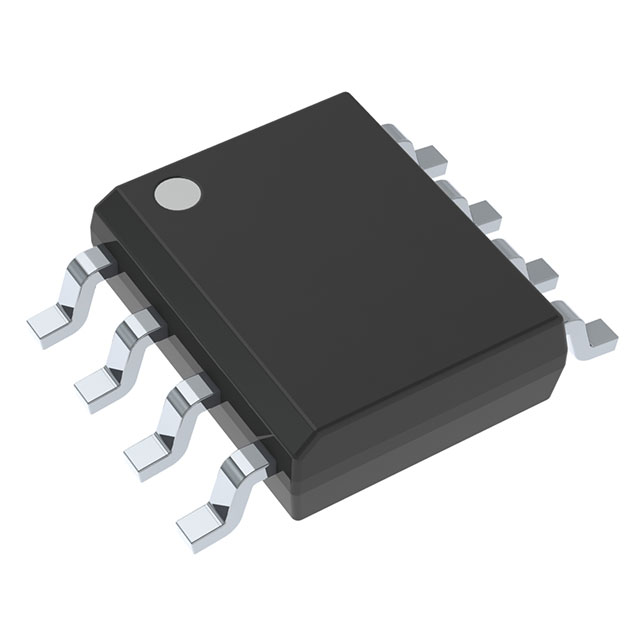
TLC27L7IDR
OP Amps, Buffer Amps ICs


.png?x-oss-process=image/format,webp/resize,p_30)


TLC27L7IDR Description
TLC27L7IDR Description
The TLC27L7IDR is a high-performance CMOS operational amplifier from Texas Instruments, designed for applications requiring low power consumption and high precision. This dual-channel amplifier is part of the LinCMOS™ series, known for its excellent performance and reliability. The TLC27L7IDR operates from a wide supply voltage range of 4 V to 16 V, making it suitable for a variety of power supply configurations. Each channel consumes only 20 µA, ensuring minimal power usage, which is ideal for battery-operated and energy-efficient designs.
TLC27L7IDR Features
- Low Power Consumption: With a supply current of just 20 µA per channel, the TLC27L7IDR is highly efficient, making it perfect for low-power applications.
- Wide Supply Voltage Range: The amplifier operates from 4 V to 16 V, providing flexibility in power supply options.
- High Input Impedance: The low input bias current of 0.6 pA ensures minimal loading on the input signal source, preserving signal integrity.
- Low Input Offset Voltage: The 170 µV input offset voltage guarantees high accuracy and precision in signal processing.
- Gain Bandwidth Product: A gain bandwidth product of 110 kHz ensures stable and accurate amplification across a wide frequency range.
- Slew Rate: The 0.03 V/µs slew rate provides smooth and controlled signal transitions, reducing distortion.
- High Output Current: Each channel can drive up to 30 mA, allowing the TLC27L7IDR to drive moderate loads directly.
- Moisture Sensitivity Level: MSL 1 (Unlimited) ensures the device is highly resistant to moisture, making it suitable for various environmental conditions.
- Compliance: The TLC27L7IDR is REACH unaffected and RoHS3 compliant, meeting stringent environmental and safety standards.
TLC27L7IDR Applications
The TLC27L7IDR is ideal for a range of applications where precision, low power, and reliability are critical. Some specific use cases include:
- Signal Conditioning: The high input impedance and low offset voltage make it suitable for conditioning weak signals in sensors and transducers.
- Battery-Powered Devices: The low power consumption ensures long battery life, making it perfect for portable and handheld devices.
- Industrial Control Systems: The wide supply voltage range and high output current capability make it suitable for industrial applications where robustness and reliability are essential.
- Medical Equipment: The precision and low power consumption are beneficial in medical devices where accuracy and energy efficiency are paramount.
- Automotive Electronics: The device's robustness and wide operating voltage range make it suitable for automotive applications where reliability and performance are crucial.
Conclusion of TLC27L7IDR
The TLC27L7IDR from Texas Instruments is a versatile and high-performance CMOS operational amplifier that offers a unique combination of low power consumption, high precision, and wide operating voltage range. Its low input bias current and low input offset voltage ensure high accuracy and signal integrity, making it suitable for a variety of applications, including signal conditioning, battery-powered devices, industrial control systems, medical equipment, and automotive electronics. The device's compliance with REACH and RoHS3 standards further enhances its suitability for modern, environmentally conscious designs. The TLC27L7IDR is an excellent choice for engineers seeking a reliable, efficient, and high-performance solution for their analog signal processing needs.
Tech Specifications
TLC27L7IDR Documents
Download datasheets and manufacturer documentation for TLC27L7IDR
 TLC27L2(A, B), TLC27L7 Datasheet
  TLC27L2(A, B), TLC27L7 Datasheet
  Design 25/Feb/2022
 Shopping Guide


.png?x-oss-process=image/format,webp/resize,h_32)


