

Texas Instruments
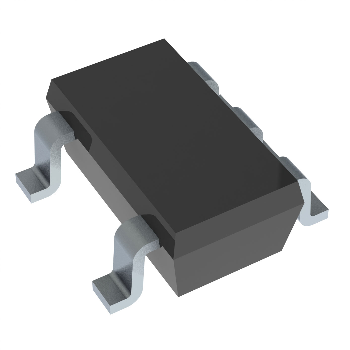
TLV2711IDBVR
OP Amps, Buffer Amps ICs

Not available to buy online? Want the lower wholesale price? Please Send RFQ to get best price, we will respond immediately


.png?x-oss-process=image/format,webp/resize,p_30)


TLV2711IDBVR Description
TLV2711IDBVR Description
The TLV2711IDBVR is a high-performance operational amplifier (op-amp) from Texas Instruments, designed for a wide range of applications in the electronics industry. This single-circuit op-amp is part of the LinCMOS™ series, offering excellent performance in a compact SOT23-5 package. With a supply voltage range of 2.7V to 10V, the TLV2711IDBVR is suitable for low-voltage applications while maintaining high performance.
TLV2711IDBVR Features
- Voltage - Supply Span (Max): 10V
- Voltage - Supply Span (Min): 2.7V
- Gain Bandwidth Product: 65 kHz
- Slew Rate: 0.025V/µs
- Current - Input Bias: 1 pA
- Current - Supply: 13µA
- Current - Output / Channel: 50 mA
- Voltage - Input Offset: 450 µV
- Mounting Type: Surface Mount
- Package: Tape & Reel (TR)
- Number of Circuits: 1
- Series: LinCMOS™
- Amplifier Type: General Purpose
- RoHS Status: ROHS3 Compliant
- REACH Status: REACH Unaffected
- Moisture Sensitivity Level (MSL): 1 (Unlimited)
- ECCN: EAR99
- HTSUS: 8542.33.0001
- Base Product Number: TLV2711
The TLV2711IDBVR stands out from similar models due to its low input bias current of 1 pA, which is ideal for applications requiring high input impedance. Its low supply current of 13µA makes it suitable for battery-powered applications. The device's 65 kHz gain bandwidth product and 0.025V/µs slew rate ensure fast response and stability in various signal processing tasks.
TLV2711IDBVR Applications
The TLV2711IDBVR is ideal for a wide range of applications, including:
- Audio Amplification: Its low noise and high slew rate make it suitable for audio preamplifiers and line drivers.
- Sensor Conditioning: The low input bias current and low offset voltage make it ideal for conditioning signals from sensors such as thermocouples and strain gauges.
- Precision Instrumentation: Its low noise and low drift characteristics are suitable for precision instrumentation and control systems.
- Battery-Powered Devices: The low supply current makes it suitable for battery-powered devices, such as portable electronics and wearables.
Conclusion of TLV2711IDBVR
The TLV2711IDBVR is a versatile and high-performance op-amp from Texas Instruments, offering excellent technical specifications and performance benefits. Its low input bias current, low supply current, and compact packaging make it ideal for a wide range of applications, including audio amplification, sensor conditioning, precision instrumentation, and battery-powered devices. With its unique features and advantages over similar models, the TLV2711IDBVR is a reliable choice for demanding electronics applications.
Tech Specifications
TLV2711IDBVR Documents
Download datasheets and manufacturer documentation for TLV2711IDBVR
Mechanical Outline Drawing TLV2711 EMI Immunity Performance Related Parts


Shopping Guide


.png?x-oss-process=image/format,webp/resize,h_32)


©2025 ERSA Electronics Corporation.