
Texas Instruments
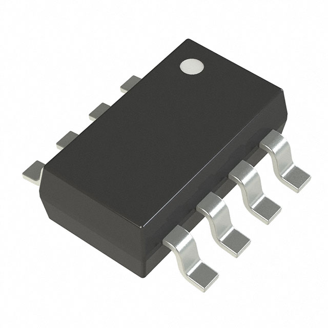
TLV3502AQDCNRQ1
Linear Comparators


- 1+
- $2.85163
- $2.85
- 10+
- $2.78539
- $27.85
- 30+
- $2.74068
- $82.22

.png?x-oss-process=image/format,webp/resize,p_30)


TLV3502AQDCNRQ1 Description
The TLV3502AQDCNRQ1 is a high-efficiency, step-down switching regulator from Texas Instruments. It is designed to provide a compact and efficient power solution for a wide range of applications.
Description:
The TLV3502AQDCNRQ1 is a highly integrated, synchronous, step-down converter with an input voltage range of 4.75V to 23V and an output voltage range of 0.9V to 5.5V. It has a wide range of features that make it suitable for use in a variety of applications, including portable devices, battery-powered equipment, and industrial systems.
Features:
- High Efficiency: The TLV3502AQDCNRQ1 offers high efficiency of up to 95%, which helps to minimize power dissipation and improve overall system performance.
- Wide Input Voltage Range: The regulator can accept input voltages from 4.75V to 23V, making it suitable for use in a wide range of applications.
- Low Output Voltage: The output voltage can be as low as 0.9V, which is ideal for powering low-voltage devices.
- High Current Capability: The TLV3502AQDCNRQ1 can deliver up to 2A of continuous output current, making it suitable for powering high-current devices.
- Small Package Size: The regulator is available in a compact QFN package, which makes it ideal for use in space-constrained applications.
- Low Dropout Voltage: The TLV3502AQDCNRQ1 has a low dropout voltage of 300mV at full load, which helps to maintain high efficiency even under low input voltage conditions.
- Protection Features: The regulator includes over-current protection, over-temperature protection, and under-voltage lockout to ensure reliable operation.
Applications:
The TLV3502AQDCNRQ1 is suitable for use in a wide range of applications, including:
- Portable Devices: The high efficiency and low dropout voltage make it ideal for use in portable devices such as smartphones, tablets, and wearable devices.
- Battery-Powered Equipment: The wide input voltage range and low output voltage make it suitable for use in battery-powered equipment such as drones, robotics, and remote sensing devices.
- Industrial Systems: The high current capability and compact package size make it suitable for use in industrial systems such as motor drives, control systems, and power supplies.
- Medical Devices: The low output voltage and high efficiency make it suitable for use in medical devices such as hearing aids, blood glucose monitors, and portable defibrillators.
Overall, the TLV3502AQDCNRQ1 is a versatile and efficient switching regulator that offers a range of features that make it suitable for use in a wide range of applications.
Tech Specifications
TLV3502AQDCNRQ1 Documents
Download datasheets and manufacturer documentation for TLV3502AQDCNRQ1
 TLV3502-Q1
  TIPD108: PWM Signal Generator
  TLV3502-Q1
 Shopping Guide


.png?x-oss-process=image/format,webp/resize,h_32)


