
 German
 Japanese
 Portuguese
 Korea
Korea
 Mexico
 Dutch
Dutch


Texas Instruments
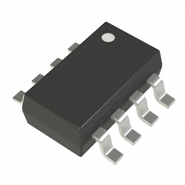
TLV9052IDDFR

Why Choose Us?
Professional Platform
B2B & B2C purchasingDelivery at full speed
1-2 days deliveryWide variety
Original manufacturers365 days guarantee
Responsible quality
.png)


Tech Specifications
TLV9052IDDFR Description
The Texas Instruments TLV9052IDDFR is a high-performance, low-power, dual-channel, 12-bit analog-to-digital converter (ADC) with a flexible input multiplexer (MUX) and a serial peripheral interface (SPI) for communication.
Description:
The TLV9052IDDFR is a precision ADC designed for use in a wide range of applications, including industrial, medical, and consumer electronics. It features a low power consumption of only 13.5 mW, making it ideal for battery-powered devices. The device has a maximum sampling rate of 200 kSPS and supports both unipolar and bipolar inputs.
Features:
- Dual-channel, 12-bit precision ADC
- Low power consumption: 13.5 mW
- Flexible input multiplexer (MUX) for selecting between two input channels
- Serial peripheral interface (SPI) for communication
- Supports unipolar and bipolar inputs
- Programmable gain amplifier (PGA) for adjusting input signal range
- Internal reference voltage for easy calibration
- Small package size: 10-lead WSON package
Applications:
- Industrial control systems: The TLV9052IDDFR can be used in industrial control systems for monitoring and controlling various parameters such as temperature, pressure, and humidity.
- Medical equipment: The device can be used in medical equipment for measuring vital signs, such as blood pressure, heart rate, and body temperature.
- Consumer electronics: The TLV9052IDDFR can be used in consumer electronics for applications like battery monitoring, temperature sensing, and humidity control.
- IoT devices: The low power consumption and high precision make the TLV9052IDDFR suitable for IoT devices that require accurate sensing and monitoring of environmental parameters.
- Automotive applications: The device can be used in automotive applications for monitoring and controlling various parameters, such as engine temperature, fuel level, and tire pressure.
In summary, the Texas Instruments TLV9052IDDFR is a versatile, low-power, dual-channel ADC with a flexible input MUX and SPI interface, making it suitable for a wide range of applications in industrial, medical, consumer electronics, IoT devices, and automotive systems.
FAQ
Not available to buy online? Want the lower wholesale price? Please Send RFQ to get best price, we will respond immediately


.png?x-oss-process=image/format,webp/resize,h_32)


