
Texas Instruments
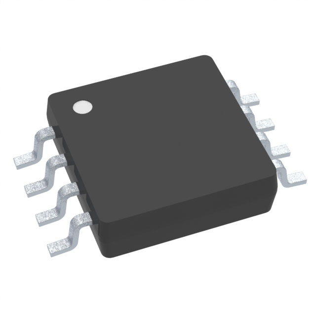
TLV9052IDGKR
OP Amps, Buffer Amps ICs


- 1+
- $0.27158
- $0.27
- 10+
- $0.26496
- $2.65
- 30+
- $0.25999
- $7.8
- 100+
- $0.25502
- $25.5

.png?x-oss-process=image/format,webp/resize,p_30)


TLV9052IDGKR Description
The TLV9052IDGKR is a high-performance, low-power, single-supply, precision operational amplifier (op-amp) from Texas Instruments. It is designed to provide excellent accuracy and low power consumption, making it suitable for a wide range of applications.
Description:
The TLV9052IDGKR is a monolithic integrated circuit that is manufactured using Texas Instruments' advanced CMOS process technology. It is available in a small-outline, wide-body SOIC-8 package, making it easy to integrate into a variety of applications.
Features:
The TLV9052IDGKR offers several features that make it an excellent choice for precision applications:
- Low Input Offset Voltage: The TLV9052IDGKR has an input offset voltage of typically 0.6 mV, which is very low compared to other op-amps. This low input offset voltage ensures high accuracy in applications that require precise amplification of small signals.
- Low Power Consumption: The TLV9052IDGKR operates from a single supply voltage of 2.7 V to 5.5 V and has a low quiescent current of 130 µA. This low power consumption makes it ideal for battery-powered applications.
- High Input Impedance: The TLV9052IDGKR has a high input impedance of 1.8 GΩ, which allows it to drive high impedance loads without significant signal degradation.
- Precision Output Stage: The TLV9052IDGKR features a precision output stage that provides low output voltage drift and excellent linearity over a wide range of output voltages.
- Rail-to-Rail Input and Output: The TLV9052IDGKR has a rail-to-rail input and output, which allows it to operate with input signals that are close to the supply rails and provides a wide output voltage range.
Applications:
The TLV9052IDGKR is suitable for a wide range of applications that require high precision and low power consumption. Some of the key applications include:
- Battery-Powered Instruments: The low power consumption and precision performance of the TLV9052IDGKR make it ideal for use in battery-powered instruments such as portable medical devices and handheld test equipment.
- Sensor Conditioning: The TLV9052IDGKR can be used to amplify and filter signals from a variety of sensors, including temperature, pressure, and strain gauges.
- Data Acquisition Systems: The TLV9052IDGKR can be used in data acquisition systems to provide precise amplification and filtering of analog signals.
- Audio Applications: The TLV9052IDGKR can be used in audio applications such as preamplifiers and active filters, where precision and low noise are critical.
- Industrial Control Systems: The TLV9052IDGKR can be used in industrial control systems to provide precise amplification and filtering of signals from sensors and other analog sources.
In summary, the TLV9052IDGKR is a high-performance, low-power, precision op-amp from Texas Instruments that offers excellent accuracy and low power consumption. Its features, such as low input offset voltage, high input impedance, and precision output stage, make it suitable for a wide range of applications, including battery-powered instruments, sensor conditioning, data acquisition systems, audio applications, and industrial control systems.
Tech Specifications
TLV9052IDGKR Documents
Download datasheets and manufacturer documentation for TLV9052IDGKR
 Additional Assembly Sites 16/Dec/2021
  TLV9051, TLV9052, TLV9054
  Marking change 01/Feb/2023
  TLV9051, TLV9052, TLV9054
  TLV905y Datasheet 3/Oct/2019
 Shopping Guide


.png?x-oss-process=image/format,webp/resize,h_32)


