
Texas Instruments
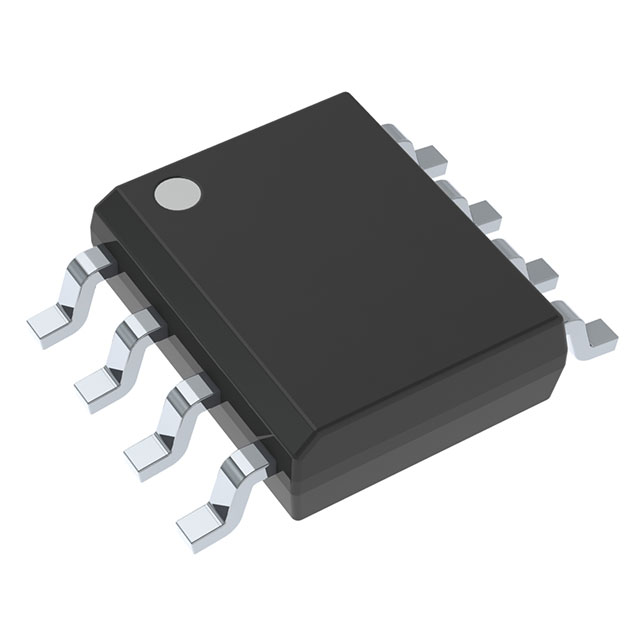
TPS1120DR
FET, MOSFET Arrays


.png?x-oss-process=image/format,webp/resize,p_30)


TPS1120DR Description
TPS1120DR Description
The TPS1120DR is a high-performance MOSFET (Metal Oxide) device from Texas Instruments, designed for applications requiring efficient power management and control. This product is part of the MOSFET Arrays category and is currently active in the market. With a maximum drain-to-source voltage (Vdss) of 15V and a continuous drain current (Id) of 1.17A at 25°C, the TPS1120DR is capable of handling demanding power requirements.
TPS1120DR Features
- Logic Level Gate: The TPS1120DR features a logic level gate, enabling compatibility with standard logic level signals for easy integration into existing systems.
- Low Gate Charge (Qg): With a maximum gate charge of 5.45nC @ 10V, the TPS1120DR reduces power dissipation and improves overall efficiency.
- Low Rds On: The maximum Rds On of 180mOhm @ 1.5A, 10V ensures low on-resistance, minimizing power losses and heat generation.
- Surface Mount Technology: The TPS1120DR is designed for surface mount applications, providing a compact and reliable solution for space-constrained designs.
- Compliance: This product is REACH Unaffected and RoHS3 Compliant, ensuring environmental and regulatory compliance.
TPS1120DR Applications
The TPS1120DR is ideal for a variety of applications where efficient power management and control are critical. Some specific use cases include:
- Power Management Systems: The TPS1120DR's low Rds On and high Vdss make it suitable for power management systems in consumer electronics, industrial equipment, and automotive applications.
- Motor Control: The device's ability to handle high currents and voltages makes it an excellent choice for motor control applications, such as in robotics and automation systems.
- Battery Protection Circuits: The TPS1120DR can be used in battery protection circuits to prevent overcharging and discharging, ensuring battery longevity and safety.
Conclusion of TPS1120DR
The TPS1120DR from Texas Instruments is a versatile MOSFET device that offers a combination of high performance, low power dissipation, and compliance with environmental regulations. Its unique features, such as the logic level gate and low Rds On, make it an ideal choice for a wide range of applications, including power management systems, motor control, and battery protection circuits. With its robust performance and reliability, the TPS1120DR is a valuable addition to any electronics design.
Tech Specifications
TPS1120DR Documents
Download datasheets and manufacturer documentation for TPS1120DR
 TPS1120, TPS1120Y
  TPS1120, TPS1120Y
  Design 25/Feb/2022
 Shopping Guide


.png?x-oss-process=image/format,webp/resize,h_32)


