
 German
 Japanese
 Portuguese
 Korea
Korea
 Mexico
 Dutch
Dutch


STGAP2SICSNTR Isolator: Description, Features, and Applications

What is an STGAP2SICSNTR?
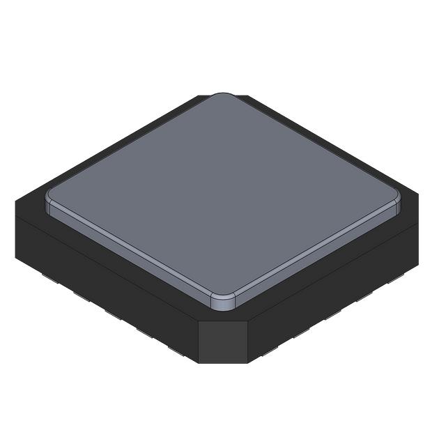
The STGAP2SICSNTR is a gate driver specifically designed for controlling high-power Silicon Carbide (SiC) MOSFETs in power electronic systems. With its focus on efficiency, it enables fast switching and low power loss in high-voltage applications. It is commonly used in sectors such as electric vehicles, industrial drives, and renewable energy systems.
.jpg?x-oss-process=image/auto-orient,1/quality,q_70/format,webp)
The STGAP2SICSNTR is part of STMicroelectronics' series of robust, high-performance gate drivers, optimized to manage the challenging demands of high-voltage switching applications. It supports high-frequency operation, which makes it ideal for applications requiring fast switching speeds to improve overall system performance.
STGAP2SICSNTR Pinout
The STGAP2SICSNTR is a gate driver IC from STMicroelectronics, specifically designed for driving silicon carbide (SiC) MOSFETs in high-power applications. Here’s a typical pinout for this component:

| Pin Number | Pin Name | Description |
| 1 | VSS | Ground (Low) |
| 2 | VDD | Supply Voltage for the IC |
| 3 | VSS2 | Second ground pin (often tied to VSS) |
| 4 | COM | Common pin for logic input and output |
| 5 | IN+ | Non-inverting input for the gate drive |
| 6 | IN- | Inverting input for the gate drive |
| 7 | FLT | Fault signal output |
| 8 | LO | Low-side driver output |
| 9 | HO | High-side driver output |
| 10 | VSS3 | Another ground pin (connected to VSS) |
Key Features of STGAP2SICSNTR
The STGAP2SICSNTR is a galvanically isolated single gate driver for SiC MOSFETs, designed to provide isolation between the gate driving channel and the low voltage control circuitry. It has a 4 A sink/source driver current capability at 25°C.
Key features of the STGAP2SICSNTR include:
- High Voltage Rail Up to 1700V
- Driver Current 4 A sink/source at 25°C
- Isolation Galvanic isolation of 4 kV
- Transient Immunity dV/dt transient immunity ±100 V/ns in full temperature range
- Propagation Delay Overall input-output propagation delay of 75 ns
- Separate Outputs Separate sink and source options for easy gate driving configuration
- Miller Clamp 4 A Miller CLAMP dedicated pin option
- UVLO Function Integrated Undervoltage lockout (UVLO) function
- Gate Driving Voltage Up to 26 V
- TTL/CMOS Inputs 3.3 V, 5 V TTL/CMOS inputs with hysteresis
- Temperature Protection Temperature shutdown protection
- Standby Function Standby function to reduce idle power consumption
The STGAP2SICSNTR is available in an SO-8 package. It operates within an industrial-grade temperature range of -40°C to 125°C. It is suitable for applications such as motor drivers, industrial drives, fans, 600/1200 V inverters, battery chargers, induction heating, welding, UPS, power supply units, and DC-DC converters.
STGAP2SICSNTR Specifications
| Parameter | Value |
| Operating Supply Voltage (VDD) | 12V to 20V |
| Low-side Output Voltage (LO) | 12V (typical) |
| High-side Output Voltage (HO) | 12V (typical) |
| Input Voltage (IN+, IN-) | 0V to 5V (typical) |
| Gate Drive Current (Source/Sink) | 1.2A / 2A (typical) |
| Propagation Delay (t_PLH/t_PHL) | 50ns (typical) |
| Under-Voltage Lockout (UVLO) | 8V (typical) for VDD, 8V for VB (high-side) |
| Output Rise Time (tr) | 20ns (typical) |
| Output Fall Time (tf) | 20ns (typical) |
| Temperature Range | -40°C to +125°C |
| Technology | CMOS |
| Gate Driver Voltage | 20V max (high-side and low-side) |
| Fault Protection | Integrated fault feedback and protection |
| Package | SO-8 |
| Application | Driving SiC MOSFETs, power MOSFETs |
Advantages of Using STGAP2SICSNTR
The STGAP2SICSNTR is a galvanically isolated single gate driver with a 4A driving capability, designed for Silicon Carbide (SiC) MOSFETs. It provides isolation between the gate driving channel and the low-voltage control circuitry.

Key advantages of using the STGAP2SICSNTR include:
High Voltage Rail: Up to 1700V.
Drive Strength: Offers a 4A sink/source current @25°C.
dV/dt transient immunity: Withstands ±100 V/ns in full temperature range.
Short Propagation Delay: Input-to-output propagation delay is around 75 ns, allowing for high PWM control accuracy.
Flexibility: Features separate sink and source options for gate driving configuration and a 4 A Miller CLAMP dedicated pin option.
Integrated Protection: Includes UVLO function and temperature shutdown protection.
CMOS/TTL compatible: Input pins are compatible with 3.3 V and 5 V TTL/CMOS with hysteresis.
Standby Mode: Includes a standby function to reduce power consumption.
Isolation: Offers 4.8 kV PK isolation.
Compact package: Available in a narrow body SO-8 package.
Applications: Suitable for motor driver inverters, power conversion, and mid to high-power applications in industrial settings15.It can be used in home appliances, factory automation, industrial drives, fans, 600/1200 V inverters, battery chargers, welding, UPS, power supply units, and DC-DC converters.
STGAP2SICSNTR Applications
The STGAP2SICSNTR is a galvanically isolated single gate driver from STMicroelectronics designed for Silicon Carbide (SiC) MOSFETs. It is suitable for mid- and high-power applications due to its 4A capability and rail-to-rail outputs. Below are some applications for STGAP2SICSNTR:
- Motor driver for home appliances, factory automation, industrial drives, and fans
- 600/1200 V inverters
- Battery chargers
- Induction heating
- Welding
- UPS
- Power supply units
- DC-DC converters
- Power Factor Correction
STGAP2SICSNTR Equivalents
| Part Number | Manufacturer | Description | Comments |
| IR2110 | Infineon | High/Low Side Driver for MOSFETs | Widely used for driving MOSFETs in power systems |
| TC4420 | Microchip | Dual High-Speed Power MOSFET Driver | Compatible with MOSFETs and IGBTs, industry-standard |
| TLP250 | Toshiba | Photocoupler for MOSFET Gate Driver | Optical isolation for high-side driving |
| UC3843 | ON Semiconductor | PWM Controller with MOSFET Driver | Common in SMPS applications |
| L6384E | STMicroelectronics | High-Side and Low-Side Driver for MOSFETs | Supports low-voltage power applications |
The STGAP2SICSNTR is a specialized MOSFET driver IC typically used for driving high and low-side MOSFETs in power electronics applications. Its equivalents, such as the IR2110 by Infineon and TC4420 by Microchip, offer similar functionalities like high-speed switching and robust driving capabilities. These alternatives often cater to power management systems, offering features like optical isolation (e.g., TLP250) or PWM control (UC3843) for precise and efficient gate control in different electronic systems. Depending on the application requirements, these ICs can serve as reliable substitutes for the STGAP2SICSNTR in various industrial and power-related circuits.
Main Differences Between STGAP2SICSN and STGAP2SICS
The STGAP2SICSN and STGAP2SICS are both single-channel gate drivers from STMicroelectronics designed for driving SiC MOSFETs, but they have some key differences:
| Feature | STGAP2SICSN | STGAP2SICS |
| High Voltage Rail | Up to 1700 V | Up to 1200 V |
| Package | Narrow-body SO-8 | Wide-body SO-8W |
| Isolation | Galvanic isolation between the gate-driving channel and low-voltage control | Galvanic isolation between the gate driving channel, and the low voltage control and interface circuitry |
| Intended Applications | Energy-conscious power systems, drives, and controllers, switched-mode power supplies, high-voltage power-factor correction (PFC), DC/DC converters, uninterruptible power supplies, solar power, motor drives, fans, factory automation, household appliances, and induction heating | Mid and high-power applications such as power conversion and motor driver inverters in industrial applications1. Equipment such as high-end home appliances, industrial drives, fans, induction heaters, welders, and UPSes. |
| Other Features | Accurate PWM control, specialized Undervoltage lockout (UVLO), a Watchdog, methods to avoid induced turn-on, and thermal shutdown protection. The input-to-output propagation time is less than 75 ns with reliable switching, thanks to common-mode transient immunity of ±100 V/ns. Designed to ensure the safe operation of SiC, providing a dedicated UVLO protection whose values are higher than the ones of the version for IGBT power transistors. |
Dual input pins that let designers determine the gate-drive signal polarity. The input circuitry is compatible with CMOS/TTL logic down to 3.3V, which allows easy interfacing with a wide variety of control ICs. The total delay is less than 75, permitting accurate pulse-width modulation (PWM) control up to high switching frequencies. Matched propagation delays between the low-voltage and high-voltage sections prevent cycle distortion and minimize energy losses. |
Both have a driver current capability of 4 A sink/source at 25°C, dV/dt transient immunity of ±100 V/ns in full temperature range, an overall input-output propagation delay of 75 ns, separate sink and source options for easy gate driving configuration, a 4 A Miller CLAMP dedicated pin option, UVLO function, gate driving voltage up to 26 V, 3.3 V, 5 V TTL/CMOS inputs with hysteresis, temperature shut-down protection, and a standby function.
Working Principle of STGAP2SICSNTR
The STGAP2SICSNTR is a galvanically isolated single-gate driver for Silicon Carbide (SiC) MOSFETs, providing isolation between the gate driving channel and the low-voltage control and interface circuitry. It has a 4A driving capability with rail-to-rail outputs, suiting it for mid- and high-power applications.
Galvanic Isolation: The STGAP2SICSN provides galvanic isolation between the gate driving channel and the low voltage control and interface circuitry.
Driver Configurations: The device is available in configurations with either separated output pins to independently optimize turn-on and turn-off using dedicated gate resistors or with a single output pin and Miller CLAMP function to prevent gate spikes during fast commutations in half-bridge topologies.
Protection Features: The device integrates protection functions such as UVLO (Undervoltage lockout) with optimized value for SiC MOSFETs and thermal shutdown to facilitate the design of high-reliability systems.
Dual Input Pins: Dual input pins allow for the selection of the control signal polarity and implementation of HW interlocking protection to prevent cross-conduction in case of controller malfunction.
Propagation Delay: The input-to-output propagation delay is contained within 75 ns, which provides high PWM control accuracy.
Standby Mode: A standby mode is available to reduce idle power consumption.
Thermal Shutdown Protection: The device includes thermal shutdown protection, forcing the device into a safe state when the junction temperature reaches the TSD temperature threshold.
UVLO Protection: Undervoltage protection is available on the VH supply pin, with a fixed hysteresis that sets the turn-off threshold to prevent intermittent operation. When the VH voltage falls below the VHoff threshold, the output buffer enters a "safe state". When the VH voltage reaches the VHon threshold, the device resumes normal operation and sets the output according to the input pins' status.
Power-Up and Power-Down: "Safe State" During power-up (VH < VHon) and power-down (VH < VHoff), the device maintains a "safe state" regardless of the input pins' values. The safe state conditions are GOFF = ON state, GON = High Impedance, and CLAMP = ON state (for STGAP2SiCSNC).
STGAP2SICSNTR Datasheet

Related Articles
- ·HBM3 vs. HBM3E: Complete Technical Comparison for AI, HPC, and Global Component Procurement
- ·How Large Language Models Work
- ·SK Hynix & Samsung: The Unprecedented HBM Expansion Race
- ·Micron 6600 ION 245TB Redefines Data Center
- ·Why Memory and Storage Define the Next Decade
- ·How Artificial Intelligence Acquires “Knowledge”
- ·How DRAM Will Change the World
- ·Why SSD Write Cache Is Crucial for AI Applications
- ·DRAM Product, Technology & Application Guide
- ·HBM4 compared to HBM4E
 FAQ
FAQ




.png?x-oss-process=image/format,webp/resize,h_32)


