
 German
 Japanese
 Portuguese
 Korea
Korea
 Mexico
 Dutch
Dutch


Why Choose Us?
Professional Platform
B2B & B2C purchasingDelivery at full speed
1-2 days deliveryWide variety
Original manufacturers365 days guarantee
Responsible quality
.png)


Tech Specifications
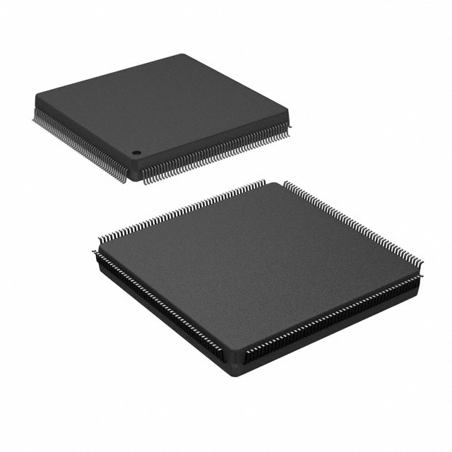
XC2S100-6PQG208C Description
The XC2S100-6PQG208C is a field programmable gate array (FPGA) device manufactured by Advanced Micro Devices (AMD). This device is part of AMD's family of programmable logic devices, which are used in a wide range of applications due to their flexibility and high performance.
Description:
The XC2S100-6PQG208C is a mid-range FPGA device that offers a balance of size, performance, and power efficiency. It is designed to provide high-speed logic functionality and can be used in a variety of applications, including digital signal processing, video processing, and communication systems.
Features:
- High-performance logic cells: The XC2S100-6PQG208C features a large number of logic cells that can be configured to perform a wide range of logic functions.
- Dedicated digital signal processing (DSP) blocks: This FPGA includes dedicated DSP blocks that can be used for high-speed mathematical operations, making it well-suited for applications that require intensive signal processing.
- High-speed I/O: The device offers a range of high-speed I/O options, including LVDS and DDR interfaces, which can be used to interface with other components in a system.
- On-chip memory: The XC2S100-6PQG208C includes a variety of on-chip memory resources, including block RAM and distributed RAM, which can be used to store data and improve system performance.
- Low power consumption: This FPGA is designed to operate at low power levels, making it suitable for applications where power efficiency is important.
Applications:
The XC2S100-6PQG208C can be used in a wide range of applications, including:
- Digital signal processing: The high-speed DSP blocks and logic cells make this FPGA well-suited for applications that require intensive signal processing, such as audio and video processing.
- Communication systems: The high-speed I/O options and flexible logic functionality make this device suitable for communication systems, including wireless base stations and network infrastructure equipment.
- Industrial control systems: The XC2S100-6PQG208C can be used in industrial control systems to implement custom logic functions and interface with various sensors and actuators.
- Automotive systems: This FPGA can be used in automotive applications, such as advanced driver assistance systems (ADAS) and infotainment systems, to provide high-speed processing and flexible I/O options.
- Test and measurement equipment: The XC2S100-6PQG208C can be used in test and measurement equipment to implement custom logic functions and interface with various instruments and sensors.
In summary, the AMD XC2S100-6PQG208C is a versatile FPGA device that offers a balance of size, performance, and power efficiency. Its features, such as high-performance logic cells, dedicated DSP blocks, and high-speed I/O options, make it suitable for a wide range of applications, including digital signal processing, communication systems, industrial control systems, automotive systems, and test and measurement equipment.
FAQ
Not available to buy online? Want the lower wholesale price? Please Send RFQ to get best price, we will respond immediately


.png?x-oss-process=image/format,webp/resize,h_32)


