
 German
 Japanese
 Portuguese
 Korea
Korea
 Mexico
 Dutch
Dutch


Why Choose Us?
Professional Platform
B2B & B2C purchasingDelivery at full speed
1-2 days deliveryWide variety
Original manufacturers365 days guarantee
Responsible quality
.png)


Tech Specifications
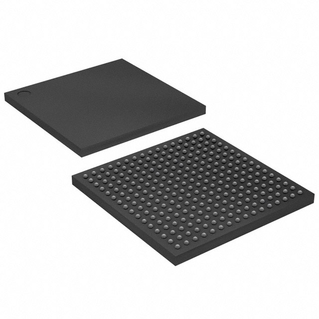
XC6SLX9-2FTG256C Description
The XC6SLX9-2FTG256C is a Field Programmable Gate Array (FPGA) device manufactured by Advanced Micro Devices (AMD). Here is a brief description of the model, its features, and potential applications:
Description:
The XC6SLX9-2FTG256C is a mid-range FPGA device from AMD's Spartan-6 family. It is designed to provide a balance between performance, power efficiency, and cost-effectiveness, making it suitable for a wide range of applications.
Features:
- Logic Density: The XC6SLX9-2FTG256C offers a high density of programmable logic resources, allowing for the implementation of complex digital circuits.
- I/O Count: It provides a substantial number of input/output (I/O) pins, facilitating connections to external devices and systems.
- Speed Grade: The "-2" in the model number indicates a speed grade of around 400 MHz, which is suitable for applications requiring moderate performance.
- Package Type: The "FTG256" denotes a flip-chip ball grid array (FCBGA) package with 256 I/Os, which is suitable for applications with space constraints or high I/O requirements.
- Power Consumption: Spartan-6 FPGAs are designed to be power-efficient, making them suitable for battery-powered or energy-sensitive applications.
- On-chip Memory: The device includes block RAM (BRAM) and distributed RAM for data storage and processing needs.
- Digital Signal Processing (DSP): It features dedicated DSP blocks for high-speed arithmetic operations, beneficial for signal processing applications.
- Interconnects and Routing: The FPGA offers a sophisticated interconnect and routing architecture, enabling efficient implementation of complex logic designs.
Applications:
- Communications: The XC6SLX9-2FTG256C can be used in communication systems, such as network routers, switches, and transceivers, due to its high I/O count and moderate speed.
- Industrial Control: It is suitable for industrial automation and control systems, where programmable logic can be used to implement custom control algorithms and interface with various sensors and actuators.
- Medical Devices: The device can be employed in medical equipment that requires real-time processing and control, such as diagnostic machines and patient monitoring systems.
- Video Processing: The FPGA can be utilized in video processing applications, including image and signal processing, due to its dedicated DSP blocks and high logic density.
- Embedded Systems: It can serve as the core processing unit in embedded systems, where custom hardware can be implemented to meet specific performance and functionality requirements.
- Aerospace and Defense: The XC6SLX9-2FTG256C can be used in aerospace and defense applications, where reliability and real-time processing are critical.
Please note that the specific features and capabilities of the XC6SLX9-2FTG256C may vary depending on the design and configuration of the FPGA. It is essential to consult the datasheet and reference materials provided by AMD for detailed information on the device's specifications and capabilities.
FAQ
| Quantity | Unit Price | Ext. Price |
|---|---|---|
| 1+ | $7.47600 | $7.48 |
| 10+ | $6.37885 | $63.79 |
| 30+ | $5.70857 | $171.26 |
| 90+ | $5.14800 | $463.32 |
Not available to buy online? Want the lower wholesale price? Please Send RFQ to get best price, we will respond immediately


.png?x-oss-process=image/format,webp/resize,h_32)


