

Not available to buy online? Want the lower wholesale price? Please Send RFQ to get best price, we will respond immediately


- 1+
- $15.21698
- $15.22
- 10+
- $14.71356
- $147.14

.png?x-oss-process=image/format,webp/resize,p_30)


XC7A15T-1FTG256C Description
XC7A15T-1FTG256C Overview
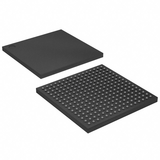
There are 170 I/Os, 1300 LABs/CLBs, and 16640 logic elements/cells on the device. The total number of RAM bits is 921600, and the voltage supply range is 0.95V to 1.05V. The XC7A15T-1FTG256C has a 256-LBGA case/package and a 256-FTBGA (17x17) supplier device package. The temperature range for operation is 0°C to 85°C (TJ). In the open market, the false danger for this product is 54%. The MSL level is 3 (for a period of 168 hours), and the REACH status is unaffected.
XC7A15T-1FTG256C Features
Wide variety of configuration options, including support for commodity memories, 256-bit AES encryption with HMAC/SHA-256 authentication, and built-in SEU detection and correction.
Low-cost, wire-bond, bare-die flip-chip, and high signal integrity flipchip packaging offering easy migration between family members in the same package. All packages available in Pb-free and selected packages in Pb option.
Designed for high performance and lowest power with 28 nm, HKMG, HPL process, 1.0V core voltage process technology and 0.9V core voltage option for even lower power.
XC7A15T-1FTG256C Applications
Consumer Electronics
Aerospace & Defense
Telecommunication
Wireless Communications
Voice recognition
Tech Specifications
XC7A15T-1FTG256C Documents
Download datasheets and manufacturer documentation for XC7A15T-1FTG256C
 7 Series FPGA Overview 7 Series FPGAs PCB Design Guide Artix-7 FPGAs Datasheet Xilinx REACH211 Cert Xiliinx RoHS Cert
 Related Parts


Relevant Search
Shopping Guide


.png?x-oss-process=image/format,webp/resize,h_32)


©2025 ERSA Electronics Corporation.