

.png?x-oss-process=image/format,webp/resize,p_30)


XC7A15T-2CSG325I Description
XC7K325T-1FB676C Overview
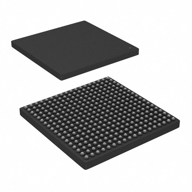
XC7K325T-1FB676C field-programmable gate array (FPGA) is a programmable logic device used for digital circuitry. With a maximum of 326,080 logic cells, this FPGA is ideal for creating sophisticated digital circuits. It also includes a maximum of 740 input/output pins for interacting with other digital devices. This FPGA requires 0.95V to 1.05V for the core voltage and 1.8V to 3.3V for the auxiliary voltage. The XC7K325T-1FB676C has an operating temperature range of -40°C to +100°C, making it appropriate for usage in a variety of settings. This FPGA is extensively utilized in aerospace, defense, and high-performance computer applications. The "FB" in the part number denotes the packaging type,which is a 676-ball fine-pitch ball grid array (FBGA). Overall, XC7K325T-1FB676C is a powerful FPGA that can be used in demanding applications that require high performance and reliability.
XC7K325T-1FB676C Features
High-speed serial connectivity with built-in multi-gigabit transceivers from 600 Mb/s to max rates of 6.6 Gb/s up to 28.05 Gb/s, offering a special low-power mode, optimized for chip-to-chip interfaces.
A user configurable analog interface (XADC), incorporating dual 12-bit 1MSPS analog-to-digital converters with on-chip thermal and supply sensors.
Powerful clock management tiles (CMT), combining phase-locked loop (PLL) and mixed-mode clock manager (MMCM) blocks for high precision and low jitter.
Quickly deploy embedded processing with MicroBlaze™ processor.
Integrated block for PCI Express® (PCIe), for up to x8 Gen3
Endpoint and Root Port designs
XC7K325T-1FB676C Applications
Consumer Electronics
Aerospace & Defense
Telecommunication
Wireless Communications
Voice recognition
Embedded Vision
Tech Specifications
XC7A15T-2CSG325I Documents
Download datasheets and manufacturer documentation for XC7A15T-2CSG325I
 7 Series FPGA Overview 7 Series FPGAs PCB Design Guide Artix-7 FPGAs Datasheet
  Xilinx REACH211 Cert Xiliinx RoHS Cert
 Relevant Search
Shopping Guide


.png?x-oss-process=image/format,webp/resize,h_32)


