

Not available to buy online? Want the lower wholesale price? Please Send RFQ to get best price, we will respond immediately


.png?x-oss-process=image/format,webp/resize,p_30)


XC7A15T-2FGG484C Description
XC7A15T-2FGG484C Overview
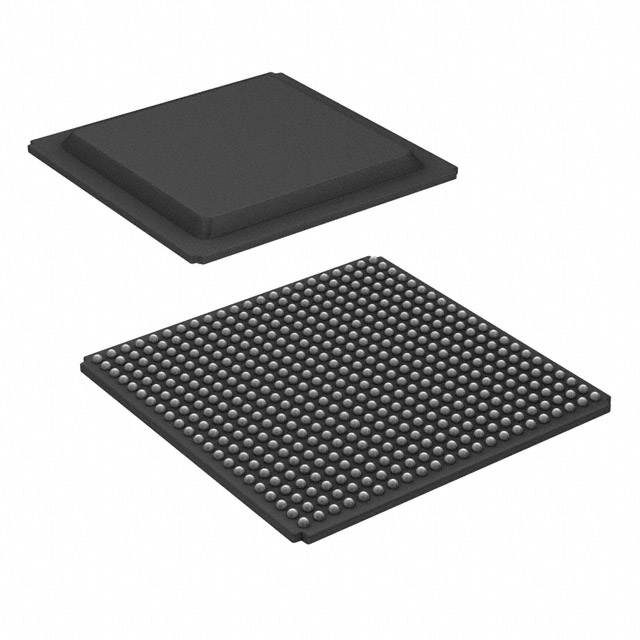
XC7A15T-2FGG484C is a field-programmable gate array (FPGA) from Xilinx, which is a programmable logic device used for digital circuitry. This FPGA has a maximum of 15,850 logic cells, which can be used to implement complex digital circuits. It also has a maximum of 210 input/output pins, which can be used to interface with other digital devices. The power requirements for this FPGA are 0.95V to 1.05V for the core voltage, and 1.8V to 3.3V for the auxiliary voltage. The operating temperature range for XC7A15T-2FGG484C is -40°C to +100°C, which makes it suitable for use in a variety of environments. This FPGA is commonly used in applications such as automotive, communications, and industrial automation. The "FGG" in the part number refers to the package type, which is a 484-ball fine-pitch ball grid array (FBGA). The "2" in the part number indicates that this FPGA is a second-generation device. Overall, XC7A15T-2FGG484C is a versatile FPGA that can be used in a wide range of applications that require moderate logic resources and I/O capabilities.
XC7A15T-2FGG484C Features
36 Kb dual-port block RAM with built-in FIFO logic for on-chip data buffering.
High-performance SelectIO™ technology with support for DDR3 interfaces up to 1,866 Mb/s.
High-speed serial connectivity with built-in multi-gigabit transceivers from 600 Mb/s to max rates of 6.6 Gb/s up to 28.05 Gb/s, offering a special low-power mode, optimized for chip-to-chip interfaces.
A user configurable analog interface (XADC), incorporating dual 12-bit 1MSPS analog-to-digital converters with on-chip thermal and supply sensors.
XC7A15T-2FGG484C Applications
Consumer Electronics
Artificial Intelligence
5G Technology
Cloud Computing
Wireless Technology
Industrial Control
Tech Specifications
XC7A15T-2FGG484C Documents
Download datasheets and manufacturer documentation for XC7A15T-2FGG484C
Related Parts


Relevant Search
Shopping Guide


.png?x-oss-process=image/format,webp/resize,h_32)


©2025 ERSA Electronics Corporation.