

Not available to buy online? Want the lower wholesale price? Please Send RFQ to get best price, we will respond immediately


- 1+
- $28.83427
- $28.83
- 30+
- $27.63367
- $829.01

.png?x-oss-process=image/format,webp/resize,p_30)


XC7A50T-2CSG324I Description
XC7A50T-2CSG324I Overview
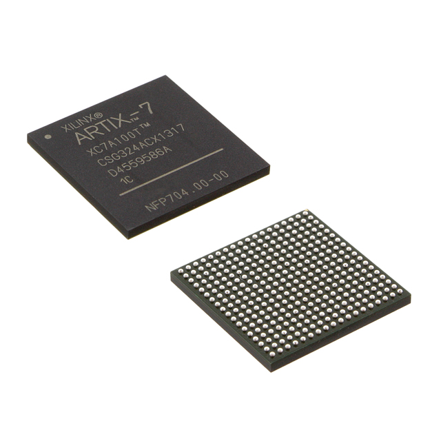
The XC7A50T-2CSG324I FPGA is intended for embedded applications requiring programmable logic capabilities. With 210 I/O pins, this FPGA provides a wide range of connectivity choices. It has 4,075 LABs/CLBs and 52,160 logic elements/cells, allowing for a wide range of designs. In addition, the gadget has 2,764,800 bits of RAM for efficient data storage and processing. The XC7A50T-2CSG324I can tolerate temperatures ranging from -40°C to 100°C while operating at a voltage range of 0.95V to 1.05V, making it appropriate for a variety of settings. It is appropriate for space-constrained applications because of its surface mount package and tiny size (15x15mm). This FPGA is an active product developed by AMD, a well-known industry provider.
XC7A50T-2CSG324I Features
High-performance SelectIO™ technology with support for DDR3 interfaces up to 1,866 Mb/s.
High-speed serial connectivity with built-in multi-gigabit transceivers from 600 Mb/s to max rates of 6.6 Gb/s up to 28.05 Gb/s, offering a special low-power mode, optimized for chip-to-chip interfaces.
A user-configurable analog interface (XADC), incorporating dual 12-bit 1MSPS analogue-to-digital converters with on-chip thermal and supply sensors.
XC7A50T-2CSG324I Applications
Communications
Automotive
Consumer Electronics
Artificial Intelligence
5G Technology
Tech Specifications
XC7A50T-2CSG324I Documents
Download datasheets and manufacturer documentation for XC7A50T-2CSG324I
 7 Series FPGA Overview Artix-7 FPGAs Datasheet Artix-7 FPGAs Brief Xilinx REACH211 Cert Xiliinx RoHS Cert
 Related Parts


Relevant Search
Shopping Guide


.png?x-oss-process=image/format,webp/resize,h_32)


©2025 ERSA Electronics Corporation.