

Lattice Semiconductor
LCMXO1200E-3FT256C
FPGAs

Not available to buy online? Want the lower wholesale price? Please Send RFQ to get best price, we will respond immediately


.png?x-oss-process=image/format,webp/resize,p_30)


LCMXO1200E-3FT256C Description
The LCMXO1200E-3FT256C is a high-performance, low-power FPGA (Field-Programmable Gate Array) device from Lattice Semiconductor. This device is part of the LatticeECP2M family, which is designed for applications that require low power, small form factor, and high performance.
Description:
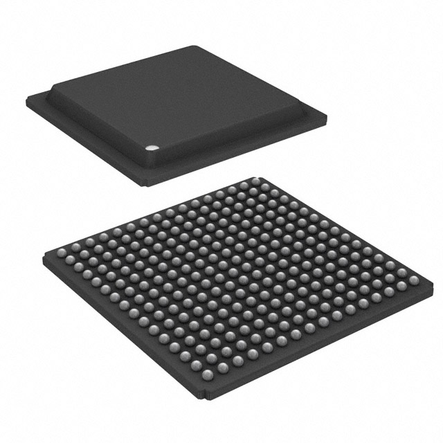
The LCMXO1200E-3FT256C is an FPGA device that is housed in a 256-ball fine-pitch ball grid array (BGA) package. It features a 3.3V power supply and a -40°C to +85°C temperature range. The device has a programmable logic array with a capacity of 1200 logic elements and 36 user I/Os.
Features:
- Low power consumption: The LCMXO1200E-3FT256C is designed for low power applications, making it ideal for battery-powered or energy-sensitive systems.
- High performance: The device offers high-speed performance with a maximum frequency of up to 400 MHz.
- Small form factor: The 256-ball BGA package allows for a compact design, making it suitable for space-constrained applications.
- Versatile I/O options: The device provides 36 user I/Os, offering flexibility in connecting to various peripherals.
- On-chip memory: The LCMXO1200E-3FT256C includes 144 Kbits of block RAM and 48 Kbits of register file memory, providing ample memory resources for various applications.
- Security features: The device offers security features such as encryption and secure boot, ensuring the protection of sensitive data and intellectual property.
- Configuration flexibility: The FPGA can be programmed and reprogrammed, allowing for easy customization and updates.
Applications:
The LCMXO1200E-3FT256C is suitable for a wide range of applications, including but not limited to:
- Industrial control systems: The device's low power consumption and high performance make it ideal for industrial automation and control applications.
- Consumer electronics: Its compact form factor and versatile I/O options make it suitable for use in consumer electronics such as smartphones, tablets, and wearable devices.
- Automotive systems: The device's temperature range and security features make it suitable for use in automotive applications, such as infotainment systems and advanced driver assistance systems (ADAS).
- Medical devices: The LCMXO1200E-3FT256C can be used in medical devices that require low power consumption, small form factor, and high performance, such as portable diagnostic equipment and monitoring systems.
- IoT devices: The device's low power consumption and flexible I/O options make it suitable for Internet of Things (IoT) applications, such as smart home devices and sensors.
- Communication systems: The high-speed performance of the LCMXO1200E-3FT256C makes it suitable for communication systems, such as base stations and routers.
In summary, the LCMXO1200E-3FT256C is a versatile, low-power FPGA device from Lattice Semiconductor that offers high performance, small form factor, and flexible I/O options. It is suitable for a wide range of applications, including industrial control systems, consumer electronics, automotive systems, medical devices, IoT devices, and communication systems.
Tech Specifications
LCMXO1200E-3FT256C Documents
Download datasheets and manufacturer documentation for LCMXO1200E-3FT256C
Alternate Foundry Site 09/Jun/2014 LCMXO_MachXO Family Datasheet All Dev Pkg Mark Chg 12/Nov/2018 Tin/Lead Devices 23/Jun/2015 LCMXO_MachXO Family Datasheet Top Mark Format Change 20/Dec/2023 Related Parts


Relevant Search
Shopping Guide


.png?x-oss-process=image/format,webp/resize,h_32)


©2025 ERSA Electronics Corporation.