

Lattice Semiconductor
LCMXO2-640HC-6SG48C
FPGAs

Not available to buy online? Want the lower wholesale price? Please Send RFQ to get best price, we will respond immediately


.png?x-oss-process=image/format,webp/resize,p_30)


LCMXO2-640HC-6SG48C Description
The Lattice Semiconductor's LCMXO2-640HC-6SG48C is a high-performance field programmable gate array (FPGA) designed for a wide range of applications. This device is part of the low-cost, low-power, and small form factor MachXO2 family, making it an ideal choice for various electronic systems.
Description:
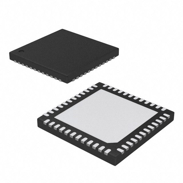
The LCMXO2-640HC-6SG48C is a 640-logic element (LE) FPGA that features a high-density architecture and a versatile set of programmable logic resources. It is available in a 6x6 mm, 48-pin surface-mount package (6SG48C), which is suitable for compact and space-constrained applications.
Features:
- Low power consumption: The device offers low static and dynamic power consumption, making it suitable for battery-powered and energy-efficient systems.
- High-performance: The LCMXO2-640HC-6SG48C provides high-speed performance with a maximum frequency of up to 400 MHz.
- Versatile I/O options: The device supports a wide range of I/O standards, including LVCMOS, SSTL, and HSTL, allowing for easy integration with various peripherals and interfaces.
- Configurable logic blocks: The FPGA features a mix of look-up tables (LUTs), flip-flops, and dedicated logic resources, enabling flexible and efficient logic implementation.
- On-chip memory: The device includes block RAM (BlockRAM) and distributed RAM, providing ample memory resources for data storage and processing.
- Digital signal processing (DSP) capabilities: The LCMXO2-640HC-6SG48C offers dedicated DSP blocks for high-speed arithmetic operations and signal processing tasks.
- Security features: The device provides security features such as encryption and secure boot to protect intellectual property and ensure system integrity.
- Easy programming: The FPGA can be easily programmed using Lattice's proprietary software development tools, such as Lattice Diamond and Lattice iCEcube2.
Applications:
The LCMXO2-640HC-6SG48C is suitable for a wide range of applications, including but not limited to:
- Industrial control and automation systems
- Communication and networking equipment
- Consumer electronics, such as set-top boxes and smart home devices
- Automotive systems, including infotainment and driver assistance systems
- Medical devices and imaging systems
- Security and surveillance systems
- Aerospace and defense applications
- IoT devices and edge computing systems
In summary, the Lattice Semiconductor's LCMXO2-640HC-6SG48C is a versatile and powerful FPGA that offers a combination of low power consumption, high performance, and a wide range of features. Its compact form factor and diverse I/O options make it suitable for various applications across different industries.
Tech Specifications
LCMXO2-640HC-6SG48C Documents
Download datasheets and manufacturer documentation for LCMXO2-640HC-6SG48C
MachXO2 Family Datasheet MachXO2 Family Handbook Product Selector Guide All Dev Pkg Mark Chg 12/Nov/2018 MachXO2 Family Handbook MachXO2™ Family Datasheet Top Mark Format Change 20/Dec/2023 Related Parts


Relevant Search
Shopping Guide


.png?x-oss-process=image/format,webp/resize,h_32)


©2025 ERSA Electronics Corporation.