

Lattice Semiconductor
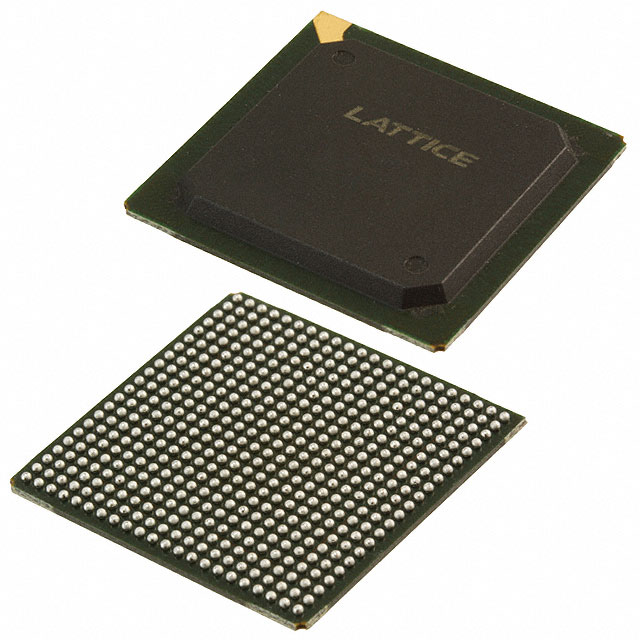
LCMXO2-7000HC-4FG484I
FPGAs

Not available to buy online? Want the lower wholesale price? Please Send RFQ to get best price, we will respond immediately


.png?x-oss-process=image/format,webp/resize,p_30)


LCMXO2-7000HC-4FG484I Description
The Lattice Semiconductor's LCMXO2-7000HC-4FG484I is a high-performance field programmable gate array (FPGA) that offers a range of features and applications for various industries.
Description:
The LCMXO2-7000HC-4FG484I is a member of Lattice Semiconductor's low-cost, low-power, and small form factor FPGA family. It is designed to provide high performance and flexibility for a wide range of applications. The device is available in a 484-ball fine-pitch ball grid array (FBGA) package, making it suitable for use in compact and space-constrained systems.
Features:
- Low Power Consumption: The LCMXO2-7000HC-4FG484I is designed to operate with low power consumption, making it ideal for battery-powered and energy-efficient applications.
- High Performance: The device offers high-speed performance, with support for high-frequency clocking and fast I/O interfaces.
- Small Form Factor: The 484-ball FBGA package allows for compact and space-efficient designs, making it suitable for use in portable and embedded systems.
- Versatility: The LCMXO2-7000HC-4FG484I is highly configurable, allowing for customization to meet the specific requirements of various applications.
- Integrated Memory: The device includes on-chip memory resources, such as block RAM and distributed RAM, to support complex data processing tasks.
- Security Features: The FPGA includes security features, such as encryption and authentication, to protect sensitive data and intellectual property.
- Development Tools: Lattice Semiconductor provides a comprehensive set of development tools, including software and hardware, to facilitate the design and implementation of custom solutions using the LCMXO2-7000HC-4FG484I.
Applications:
The LCMXO2-7000HC-4FG484I is suitable for a wide range of applications, including:
- Industrial Control Systems: The device can be used in industrial control systems for motor control, sensor interfacing, and data acquisition.
- Communication Systems: The high-speed performance and I/O interfaces make it suitable for communication systems, such as Ethernet switches and serializers/deserializers.
- Consumer Electronics: The low power consumption and small form factor make it ideal for use in portable consumer electronics, such as wearable devices and smartphones.
- Automotive Systems: The device can be used in automotive systems for infotainment, driver assistance, and safety applications.
- Medical Devices: The LCMXO2-7000HC-4FG484I can be used in medical devices for signal processing, imaging, and monitoring applications.
- Security Systems: The security features of the FPGA make it suitable for use in security systems, such as encryption and authentication applications.
- Aerospace and Defense: The device can be used in aerospace and defense applications for signal processing, communication, and control systems.
In summary, the Lattice Semiconductor's LCMXO2-7000HC-4FG484I is a versatile and high-performance FPGA that offers low power consumption, small form factor, and a range of features suitable for various applications across different industries.
Tech Specifications
LCMXO2-7000HC-4FG484I Documents
Download datasheets and manufacturer documentation for LCMXO2-7000HC-4FG484I
Alternate Assembly Revision B 17/Nov/2014 MachXO2 Family Datasheet Package Diagrams Product Selector Guide All Dev Pkg Mark Chg 12/Nov/2018 I2C Read-Back Failure Feb/2015 MachXO2™ Family Datasheet Datasheet Chg 21/Mar/2016 Top Mark Format Change 20/Dec/2023 Related Parts


Relevant Search
Shopping Guide


.png?x-oss-process=image/format,webp/resize,h_32)


©2025 ERSA Electronics Corporation.