
Lattice Semiconductor
LFEC3E-3TN100C
FPGAs


.png?x-oss-process=image/format,webp/resize,p_30)


LFEC3E-3TN100C Description
Lattice Semiconductor's LFEC3E-3TN100C is a low-cost, low-power FPGA (Field Programmable Gate Array) device designed for a wide range of applications. This device offers a combination of features that make it an ideal choice for various electronic systems.
Description:
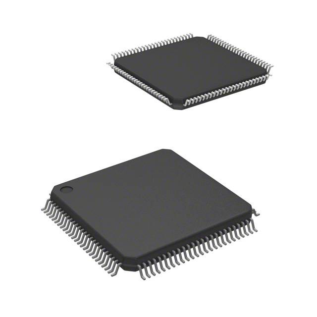
The LFEC3E-3TN100C is a member of Lattice Semiconductor's EC family of FPGAs. It is a compact, 3.3V device that comes in a 100-pin TQFP (Thin Quad Flat Package) package. This FPGA is designed to provide high performance and low power consumption, making it suitable for a wide range of applications.
Features:
- Low Power Consumption: The LFEC3E-3TN100C is designed to operate at low power levels, making it an ideal choice for battery-powered or energy-sensitive applications.
- High Performance: This FPGA offers high performance and fast processing capabilities, allowing it to handle complex tasks and algorithms efficiently.
- Versatile I/O: The device features a wide range of I/O options, including LVCMOS, LVDS, and TTL, making it suitable for interfacing with various peripherals and systems.
- Configurable Logic Blocks: The LFEC3E-3TN100C provides a high number of configurable logic blocks, allowing users to implement custom logic functions and designs.
- Embedded Memory: This FPGA includes on-chip memory resources, such as block RAM and distributed RAM, which can be used for data storage and processing.
- Integrated DSP Blocks: The device features integrated digital signal processing (DSP) blocks, which can be used for implementing various signal processing algorithms and functions.
- Security Features: The LFEC3E-3TN100C includes security features, such as encryption and authentication, to protect sensitive data and intellectual property.
Applications:
The LFEC3E-3TN100C FPGA is suitable for a wide range of applications, including but not limited to:
- Industrial Control Systems: The device's low power consumption and high performance make it ideal for use in industrial control systems, where reliability and efficiency are crucial.
- Consumer Electronics: The LFEC3E-3TN100C can be used in various consumer electronics, such as smartphones, tablets, and smart home devices, for implementing custom functions and features.
- Automotive Systems: This FPGA is suitable for use in automotive systems, such as infotainment systems, advanced driver assistance systems (ADAS), and body control modules.
- Networking and Communications: The LFEC3E-3TN100C can be used in networking and communication systems, such as routers, switches, and base stations, for implementing custom protocols and algorithms.
- Signal Processing: The integrated DSP blocks and versatile I/O options make this FPGA suitable for various signal processing applications, such as audio processing, image processing, and data acquisition systems.
- Security Systems: The security features of the LFEC3E-3TN100C make it suitable for use in security systems, such as encryption devices, secure communication systems, and access control systems.
In summary, Lattice Semiconductor's LFEC3E-3TN100C is a versatile, low-cost, and low-power FPGA that offers a wide range of features and applications, making it an ideal choice for various electronic systems and designs.
Tech Specifications
LFEC3E-3TN100C Documents
Download datasheets and manufacturer documentation for LFEC3E-3TN100C
 ECP, EC Family Package Diagrams Leaded Pkg PCB Layout Guide
  All Dev Pkg Mark Chg 12/Nov/2018
  LatticeEC/P and LatticeXP Devices 25/Jul/2013
  ECP, EC Family
  Top Mark Format Change 20/Dec/2023
 Relevant Search
Shopping Guide


.png?x-oss-process=image/format,webp/resize,h_32)


