

Microchip Technology
ATMEGA168-20MU
Microcontrollers

Not available to buy online? Want the lower wholesale price? Please Send RFQ to get best price, we will respond immediately


.png?x-oss-process=image/format,webp/resize,p_30)


ATMEGA168-20MU Description
Microchip Technology's ATMEGA168-20MU is a low-power, high-performance 8-bit microcontroller unit (MCU) that belongs to the AVR Enhanced series. It is designed to provide a cost-effective solution for a wide range of applications, including industrial control, medical devices, and consumer electronics.
Description:
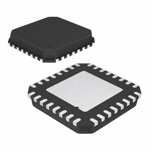
The ATMEGA168-20MU is a microcontroller based on the AVR architecture, featuring a high-speed 20 MHz clock frequency. It is housed in a 32-pin, 0.3-inch (8mm) wide, 4.9mm high, and 1.5mm pitch, QFN (Quad Flat No-leads) package. The package is designed for surface-mount technology (SMT) and offers a compact form factor suitable for space-constrained applications.
Features:
- CPU: 8-bit AVR RISC-based microcontroller with a 20 MHz clock frequency.
- Memory:
- 16 KB of In-System Programmable (ISP) Flash memory for program storage.
- 1 KB of EEPROM for non-volatile data storage.
- 1 KB of SRAM for temporary data storage.
- I/O: 14 digital I/O pins with support for various I/O modes, including PWM, ADC, and digital communication interfaces like SPI, TWI, and USART.
- ADC: 8-channel, 10-bit Analog-to-Digital Converter (ADC) with a maximum conversion rate of 100 ksps (kilo samples per second).
- Communication Interfaces: Serial Peripheral Interface (SPI), Two-Wire Interface (TWI), and Universal Synchronous/Asynchronous Receiver/Transmitter (USART).
- Timers: 2 independent 8-bit Timer/Counters with PWM and Input Capture/Output Compare modes.
- Interrupts: 15 interrupt sources, including external interrupts, timer interrupts, and I/O pin change interrupts.
- Power Management: Sleep mode, Power Reduction Register (PRR), and Brown Out Detector (BOD) for energy-efficient operation.
- Security: JTAG interface for debugging and programming, with an option to disable it for added security.
- Operating Voltage: 1.8V to 5.5V.
- Operating Temperature Range: -40°C to +85°C.
Applications:
- Industrial control systems: Programmable logic controllers, motor control, and sensor interfacing.
- Medical devices: Glucose meters, blood pressure monitors, and portable diagnostic equipment.
- Consumer electronics: Home automation, portable gaming devices, and smart appliances.
- Automotive applications: Instrumentation, infotainment systems, and body control modules.
- Telecommunications: Modems, routers, and other network devices.
- Energy management: Smart meters, energy monitoring systems, and lighting control.
- Security systems: Access control, intrusion detection, and surveillance cameras.
The ATMEGA168-20MU is a versatile and efficient microcontroller suitable for a wide range of applications that require low power consumption, high performance, and a compact form factor.
Tech Specifications
ATMEGA168-20MU Documents
Download datasheets and manufacturer documentation for ATMEGA168-20MU
View in Development Tools Selector Change from Gold to Copper Bonding Wire (PDF) Convert MSL3 to MSL1 for QFN Packages (PDF) Product Change Notification 2024-03-04 (PDF) Product Change Notification to add wafer fabrication facility (PDF) Product Change Notification (PDF) ATMEGA168-20MU Symbol & Footprint by SnapMagic Related Parts


Relevant Search
Shopping Guide


.png?x-oss-process=image/format,webp/resize,h_32)


©2025 ERSA Electronics Corporation.