
 German
 Japanese
 Portuguese
 Korea
Korea
 Mexico
 Dutch
Dutch


Microchip Technology
ATMEGA324PB-AU

Why Choose Us?
Professional Platform
B2B & B2C purchasingDelivery at full speed
1-2 days deliveryWide variety
Original manufacturers365 days guarantee
Responsible quality
.png)


Tech Specifications
ATMEGA324PB-AU Description
The ATMEGA324PB-AU is a microcontroller unit (MCU) produced by Microchip Technology. It belongs to the ATmega family of 8-bit AVR microcontrollers, which are widely used in various embedded systems and applications due to their high performance, low power consumption, and ease of use.
Description:
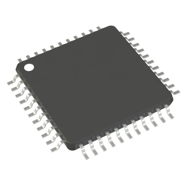
The ATMEGA324PB-AU is a high-performance, low-power 8-bit AVR microcontroller with 32 KB of In-System Programmable Flash memory, featuring a rich set of communication interfaces, timers, and other peripherals. It operates at a maximum frequency of 16 MHz and is available in a 44-pin TQFP (Thin Quad Flat Package) package.
Features:
- 32 KB of In-System Programmable Flash memory
- 2 KB of In-System Programmable SRAM
- 1 KB of EEPROM
- 44 general-purpose I/O lines
- 33 extended I/O lines
- 2 USARTs (Universal Synchronous/Asynchronous Receiver/Transmitter) with multi-purpose clock generator
- SPI (Serial Peripheral Interface) for communication with external SPI devices
- TWI (Two-Wire Interface) for communication with external I2C devices
- 8-channel 10-bit ADC (Analog-to-Digital Converter) with up to 11 single-ended or 6 differential inputs
- 6-channel PWM (Pulse Width Modulation) with phase-correct and frequency modulation modes
- 2 16-bit Timer/Counters with PWM and Input Capture modes
- 1 8-bit Timer/Counter with PWM and Input Capture modes
- 2 8-bit Timer/Counters with Input Capture mode
- 2-wire serial interface for system programming and data communication
- Internal and external Interrupt sources
- On-chip debug support with JTAG (Joint Test Action Group) interface
- Brownout detection and reset
- Power-on reset
- Clock output on pin
- Sleep mode for low-power consumption during idle periods
Applications:
The ATMEGA324PB-AU is suitable for a wide range of applications due to its versatile features and communication interfaces. Some common applications include:
- Industrial control systems
- Home automation and smart home devices
- Medical equipment and monitoring systems
- Automotive control systems
- Robotics and automation
- Data acquisition and signal processing systems
- Communication and networking devices
- Consumer electronics, such as appliances and portable devices
- Security systems and access control
- Embedded systems in IoT (Internet of Things) devices
The ATMEGA324PB-AU's combination of performance, low power consumption, and a wide range of communication interfaces make it an ideal choice for developers looking to create efficient and reliable embedded systems.
FAQ
| Quantity | Unit Price | Ext. Price |
|---|---|---|
| 1+ | $1.96240 | $1.96 |
| 25+ | $1.80400 | $45.10 |
| 100+ | $1.62800 | $162.80 |
Not available to buy online? Want the lower wholesale price? Please Send RFQ to get best price, we will respond immediately


.png?x-oss-process=image/format,webp/resize,h_32)


