

NXP Semiconductors
LPC1114FDH28/102:5
Microcontrollers

Not available to buy online? Want the lower wholesale price? Please Send RFQ to get best price, we will respond immediately


.png?x-oss-process=image/format,webp/resize,p_30)


LPC1114FDH28/102:5 Description
NXP Semiconductors' LPC1114FDH28/102:5 is a low-cost, low-power microcontroller unit (MCU) belonging to the LPC110x family. It is designed for a wide range of applications, including industrial, medical, and consumer electronics. Here's a detailed description, features, and applications of the LPC1114FDH28/102:5:
Description:
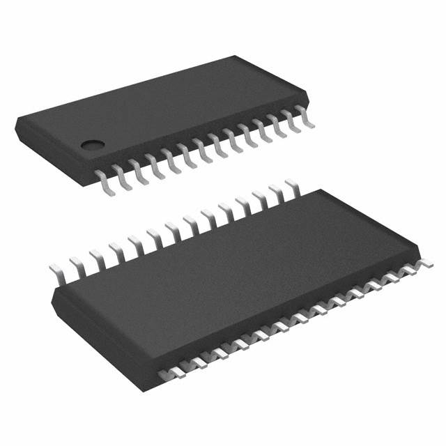
The LPC1114FDH28/102:5 is a 32-bit ARM Cortex-M0-based MCU with 16 kB to 128 kB of on-chip Flash memory and 4 kB to 16 kB of on-chip RAM. It operates at a core frequency of up to 50 MHz, providing high performance with low power consumption. The device is available in a 28-pin QFN package.
Features:
- ARM Cortex-M0 processor core with a core frequency of up to 50 MHz.
- Memory options: 16 kB to 128 kB of on-chip Flash memory and 4 kB to 16 kB of on-chip RAM.
- GPIO (General Purpose Input/Output) pins with various functions, such as digital I/O, analog inputs, and communication interfaces.
- Support for multiple communication protocols, including I2C, SPI, and UART (Universal Asynchronous Receiver/Transmitter).
- Up to 8-channel 10-bit ADC (Analog-to-Digital Converter) for converting analog signals to digital values.
- PWM (Pulse Width Modulation) channels for generating precise control signals.
- WDT (Watchdog Timer) for system monitoring and reset functionality.
- RTC (Real-Time Clock) for timekeeping and alarms.
- Low-power modes, such as Sleep and Deep Sleep, to conserve energy during periods of inactivity.
- On-chip oscillator with an accuracy of ±1% over temperature and supply voltage.
- Small form factor (28-pin QFN package) for space-constrained applications.
Applications:
- Industrial control and automation systems.
- Medical devices, such as portable monitoring equipment and diagnostic tools.
- Consumer electronics, including portable devices, smart home appliances, and wearables.
- Battery-powered devices, where low power consumption is crucial.
- Sensor interfaces and data acquisition systems.
- Human Interface Devices (HIDs), such as keyboards, mice, and touchpads.
- Simple embedded control systems for various applications, such as motor control and lighting control.
The LPC1114FDH28/102:5 is a versatile and cost-effective solution for a wide range of embedded applications, offering a balance of performance, power efficiency, and features in a compact package.
Tech Specifications
LPC1114FDH28/102:5 Documents
Download datasheets and manufacturer documentation for LPC1114FDH28/102:5
LPC1110-15 All Dev Label Update 15/Dec/2020 Mult Dev Pkg Seal 15/Dec/2020 OM13314,598: Power Line Lighting Control LPC1110-15 NXP USA Inc REACH NXP USA Inc RoHS Cert Related Parts


Shopping Guide


.png?x-oss-process=image/format,webp/resize,h_32)


©2025 ERSA Electronics Corporation.