

onsemi
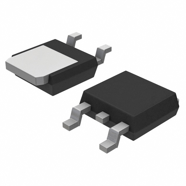
FDD9409-F085
Single FETs, MOSFETs

Not available to buy online? Want the lower wholesale price? Please Send RFQ to get best price, we will respond immediately


- 1+
- $1.23070
- $1.23
- 10+
- $1.20290
- $12.03
- 30+
- $1.18440
- $35.53

.png?x-oss-process=image/format,webp/resize,p_30)


FDD9409-F085 Description
FDD9409-F085 Description
The FDD9409-F085 is a high-performance MOSFET N-CH 40V 90A DPAK from onsemi, designed for automotive applications. This MOSFET is built using the advanced PowerTrench® technology, ensuring superior performance and reliability. With a maximum drain-source voltage of 40V and a continuous drain current of 90A at 25°C, the FDD9409-F085 is ideal for high-power applications.
FDD9409-F085 Features
- Input Capacitance (Ciss): 3130 pF @ 25 V, ensuring fast switching speeds and reduced power consumption.
- Gate Charge (Qg): 46 nC @ 10 V, minimizing gate charge and improving efficiency.
- Drain to Source Voltage (Vdss): 40 V, suitable for high-voltage applications.
- Power Dissipation (Max): 150W (Tc), allowing for high-power operation.
- Technology: MOSFET (Metal Oxide), providing excellent electrical performance and reliability.
- Rds On (Max) @ Id, Vgs: 3.2mOhm @ 80A, 10V, ensuring low on-resistance and high efficiency.
- Vgs(th) (Max) @ Id: 4V @ 250µA, providing stable and predictable threshold voltage.
- Mounting Type: Surface Mount, suitable for compact and space-constrained designs.
- REACH Status: REACH Unaffected, ensuring compliance with European regulations.
- RoHS Status: ROHS3 Compliant, adhering to environmental standards.
- Moisture Sensitivity Level (MSL): 1 (Unlimited), allowing for flexible storage and handling.
FDD9409-F085 Applications
The FDD9409-F085 is ideal for a wide range of high-power automotive applications, including:
- Battery Management Systems: Utilizing its high current and voltage capabilities, the FDD9409-F085 can efficiently manage battery charging and discharging.
- Power Converters: Its low on-resistance and high efficiency make it suitable for power conversion applications, such as DC-DC converters.
- Motor Controls: The FDD9409-F085 can effectively control high-power motors in electric vehicles and other automotive systems.
Conclusion of FDD9409-F085
The FDD9409-F085 is a powerful and reliable MOSFET designed for high-performance automotive applications. Its advanced PowerTrench® technology, combined with its superior electrical characteristics, make it an excellent choice for demanding power management and control systems. While it is not recommended for new designs, the FDD9409-F085 remains a strong contender in existing automotive applications where its unique features and advantages are required.
Tech Specifications
FDD9409-F085 Documents
Download datasheets and manufacturer documentation for FDD9409-F085
Mult Device Part Number Chg 30/May/2017 Mult Dev A/T 18/Aug/2021 FDD9409_F085 Mult Devices 24/Oct/2017 On Semiconductor Automotive F085 Status Check Logo 17/Aug/2017 onsemi RoHS Material Declaration FDD9409-F085 Related Parts


Shopping Guide


.png?x-oss-process=image/format,webp/resize,h_32)


©2025 ERSA Electronics Corporation.