

onsemi
FDMC86340ET80
Single FETs, MOSFETs

Not available to buy online? Want the lower wholesale price? Please Send RFQ to get best price, we will respond immediately


.png?x-oss-process=image/format,webp/resize,p_30)


FDMC86340ET80 Description
FDMC86340ET80 Description
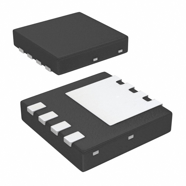
The FDMC86340ET80 from onsemi is a high-performance N-channel MOSFET utilizing advanced PowerTrench® technology, designed for efficient power management in demanding applications. With a drain-to-source voltage (Vdss) of 80V and a continuous drain current (Id) of 14A (Ta) / 68A (Tc), this MOSFET delivers robust performance in both ambient and controlled thermal environments. Its low on-resistance (Rds(on)) of 6.5mΩ at 10V Vgs ensures minimal conduction losses, making it ideal for high-efficiency power conversion. Packaged in Power33 (3.3mm x 3.3mm), it offers a compact footprint for space-constrained designs while maintaining excellent thermal dissipation.
FDMC86340ET80 Features
- Low Rds(on): 6.5mΩ @ 10V Vgs reduces power losses and improves efficiency.
- High Current Handling: 68A (Tc) capability supports high-power applications.
- Fast Switching: Low gate charge (Qg) of 49nC @ 10V and input capacitance (Ciss) of 2775pF @ 40V enable rapid switching for high-frequency designs.
- Robust Voltage Ratings: Vdss of 80V and Vgs(max) of ±20V ensure reliability under varying conditions.
- Thermal Efficiency: Power dissipation of 65W (Tc) allows sustained performance in thermally challenging environments.
- Compact Package: Power33 surface-mount package optimizes board space without compromising thermal performance.
- Compliance: ROHS3, REACH Unaffected, and ECCN EAR99 certified for global use.
FDMC86340ET80 Applications
This MOSFET is particularly suited for:
- DC-DC Converters: High efficiency and low Rds(on) make it ideal for synchronous buck/boost converters.
- Motor Drives: Robust current handling supports brushed/brushless motor control in industrial and automotive systems.
- Power Supplies: Used in SMPS (Switched-Mode Power Supplies) for servers, telecom, and computing infrastructure.
- Battery Management Systems (BMS): Efficient power switching in electric vehicles (EVs) and energy storage solutions.
- Load Switches: Fast switching and low conduction losses benefit high-current load switching applications.
Conclusion of FDMC86340ET80
The FDMC86340ET80 stands out as a high-efficiency, high-reliability MOSFET for modern power electronics. Its low Rds(on), high current capability, and compact Power33 package make it a superior choice for applications demanding minimal power loss, thermal resilience, and space efficiency. Whether in DC-DC conversion, motor control, or high-density power systems, this MOSFET delivers performance that meets the stringent requirements of industrial, automotive, and telecom applications. Its compliance with global standards further ensures seamless integration into diverse designs.
Tech Specifications
FDMC86340ET80 Documents
Download datasheets and manufacturer documentation for FDMC86340ET80
Mult Dev Assembly 11/Mar/2020 FDMC86340ET80 Mult Devices 24/Oct/2017 Logo 17/Aug/2017 onsemi RoHS Material Declaration FDMC86340ET80 Related Parts


Shopping Guide


.png?x-oss-process=image/format,webp/resize,h_32)


©2025 ERSA Electronics Corporation.