
 German
 Japanese
 Portuguese
 Korea
Korea
 Mexico
 Dutch
Dutch


onsemi
NSS40300DDR2G

Why Choose Us?
Professional Platform
B2B & B2C purchasingDelivery at full speed
1-2 days deliveryWide variety
Original manufacturers365 days guarantee
Responsible quality
.png)


Tech Specifications
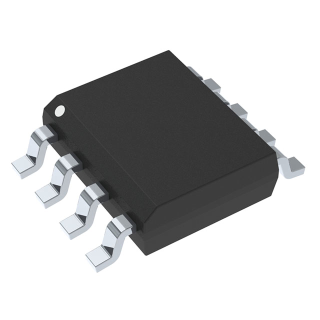
NSS40300DDR2G Description
NSS40300DDR2G Description
The NSS40300DDR2G from onsemi is a high-performance dual PNP bipolar transistor array designed for precision switching and amplification applications. Packaged in an 8-SOIC surface-mount configuration, it offers a compact footprint while delivering robust performance with a 40V collector-emitter breakdown voltage and 3A maximum collector current. Its low Vce saturation voltage (170mV @ 2A) ensures minimal power loss, making it highly efficient for power management tasks. The device is RoHS3 compliant and REACH unaffected, meeting stringent environmental and regulatory standards.
NSS40300DDR2G Features
- Dual PNP Configuration: Integrates two matched PNP transistors in a single package, saving board space and simplifying design.
- High Current Handling: Supports up to 3A continuous collector current, ideal for driving loads in power circuits.
- Low Saturation Voltage: 170mV @ 2A reduces heat dissipation and improves efficiency.
- High DC Current Gain (hFE): 180 @ 1A, 2V ensures reliable amplification in signal processing.
- Wide Operating Frequency: 100MHz transition frequency suits high-speed switching applications.
- Robust Packaging: Tape & Reel (TR) for automated assembly, with MSL 1 (Unlimited) moisture sensitivity for easy handling.
NSS40300DDR2G Applications
This transistor array excels in:
- Power Management: DC-DC converters, voltage regulators, and load switches due to its low Vce and high current capability.
- Motor Control: Driver stages for small motors or solenoids where efficient switching is critical.
- Audio Amplification: Low-distortion signal amplification in portable audio devices.
- Industrial Automation: Relay drivers and sensor interfaces requiring high reliability.
- Automotive Systems: Suitable for non-critical 12V/24V applications, adhering to robust performance standards.
Conclusion of NSS40300DDR2G
The NSS40300DDR2G stands out for its high current capacity, low saturation voltage, and compact dual-PNP integration, making it a versatile choice for modern electronics. Its surface-mount design, compliance with environmental regulations, and broad applicability in power, audio, and industrial systems position it as a superior alternative to discrete transistors. Engineers will appreciate its balance of performance, efficiency, and space-saving benefits in densely populated PCB designs.
FAQ
Not available to buy online? Want the lower wholesale price? Please Send RFQ to get best price, we will respond immediately


.png?x-oss-process=image/format,webp/resize,h_32)


